Introduction
CeBIT earlier this year was the first time we saw NVIDIA MCP73 out in the wild. The single-chip core logic, containing a brand new integrated graphics core and all traditional north and southbridge functionality needed for a modern Core 2-supporting PC platform, signaled NVIDIA's intent to go after the mainstream computing platform. Combining all core logic functionality and an IGP into one dice lets mainboard vendors create simpler and cheaper designs, while still retaining a rich plethora of features.
We've known that the IGP component would be based on NVIDIA's last generation D3D9-level technology that underpins their GeForce 7-series designs, and we've known the feature set, so there's not much new to learn today. This article therefore serves as a quick refresher, fleshing out the final details of the product line based around MCP73, before a look at couple of reference mainboard pics to get a feel for what shipping designs from NVIDIA's partners will be like.
It's worth remembering that this is NVIDIA's first IGP for Intel processors in their history. One of the artifacts of the AMD/ATI merger is that ATI won't play in that space any more, leaving NVIDIA to duke it out with Intel and SiS for marketshare (VIA's license has expired and they will no longer be able to sell their Intel chipsets as of April 2008).With MCP73, they've certainly got a chance. Here's why.
MCP73 Basic Specification
IGP Portion
The IGP portion of the MCP73 die contains a DX9-level GeForce 7-series GPU with 2/2/2 VS/PS/ROP configuration (about half as able than G72), with 500MHz-630MHz clock, feeding into a display controller which supports two protected (via HDCP) digital outputs, one of them HDMI, with DACs for analogue support if needed by the display. The IGP's connection to the MCP73 memory controller is undocumented, but NVIDIA make note that even with just one channel of installed system memory, the MCP73 can generate a (Windows Experience Index) WEI score that certifies it as Vista Premium compliant.
That hints that the internal IGP-MC (memory controller) connection is wide and efficient, allowing the graphics core to make the best use of installed system memory, which it has to use for all rendering ops. There's no local framebuffer memory for MCP73 to use, before spilling to system memory. It is also certainly worth pointing out that 500-630MHz is much higher than NVIDIA's equivalent IGPs for AMD platforms (the 90nm MCP68) at 425MHz.
The display controller also supports HD component output, for those looking to use MCP73-based systems in their media centre PCs, which leads us nicely on to the incorporation into the MCP73 logic of NVIDIA PureVideo technology, for acceleration assistance and image quality improvements for the playback of video based on popular codecs.
The display controller only supports single-link DVI output, but that's enough for a full 1080p digital connection.
Northbridge Portion
MCP73 provides all the logic for traditional northbridge functionality too, including a single-channel DDR2-800 memory controller, support for 1333MHz Core 2 Duo and Core 2 Quad processors from Intel, and a PCI Express Gen1 root host with 18 lane provision. The memory controller is tweaked versus what you'll find in NVIDIA's nForce 5xxi and 6xxi SPPs for their other Intel-supporting product ranges, mostly in order to best support the IGP component.
18 lanes of PCIe mean you'll almost always find one x16 and two x1 slots on MCP73 mainboards, and indeed we haven't seen a final MCP73 design that doesn't provide those expansion possibilities via PCI Express. That's not to say you won't see anyone drop a x1 (or even the x16) slot, but we haven't seen it yet.
Southbridge Portion
The I/O processor or southbridge has traditionally been where core logic products differentiate themselves from in-house competition and that from other vendors. MCP73 doesn't move the game on any from the level of feature integration we've seen from NVIDIA products in the past, but it does (almost) match it, and that means features ahoy.
MCP73 provides four SATA2 ports for hard or optical drives, two IDE ports for legacy hard or optical drives (something Intel's own core logic doesn't provide these days), ten ports of USB2.0, a legacy PCIc controller with up to 5 connected slots, a GigE port with all of NVIDIA's offload and firewall business, and finally a HD Audio controller. Deep breath.
It all adds up to one of the most feature-rich IGP platforms available, and certainly the most performant and feature-rich single-chip PC core logic yet created. Only SiS get close with one chip for Intel CPUs, and Intel need one of their ICH I/O processors along with an IGP-sporting MCH to provide the same rough level of features.
MCP73 Discussion
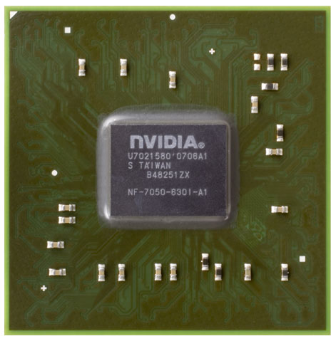
MCP73 is an 85-100mm² die (much smaller than the ~135mm² die we saw at CeBIT, which definitely wasn't MCP73, oops - it seems real chips only surfaced at Computex) built using TSMC's 80nm process. Given the level of integration, we presume NVIDIA are more than happy with the area/feature/performance tradeoffs they had to make to produce the single-chip core logic. At up to 630MHz clock for the IGP portion, it's not an insignificant endeavour to produce a mixed logic (there are analogue portions) die containing so much, at high frequencies.
The graphics core supports all the DX9-level features that existing NVIDIA GeForce 7-series products do, including full Shader Model 3.0 support for vertex and fragment processing, and NVIDIA clock parts down and disable features and support in order to create the multiple MCP73 products.
We'll discuss those on the next page.