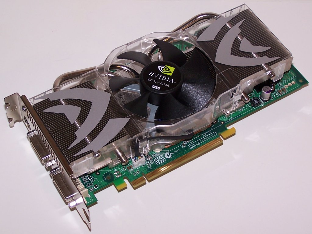
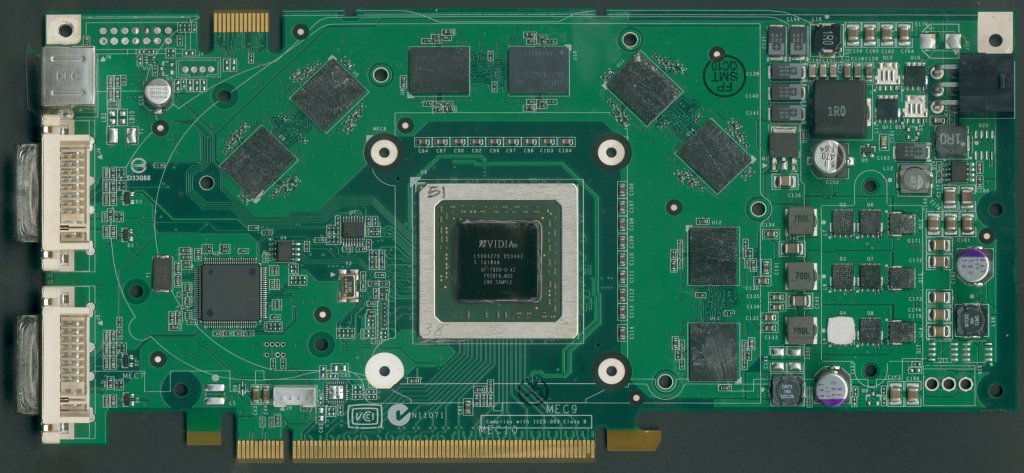
The BoardHere is a closer look at the specifications of the new GeForce 7800 GTX 512MB board and a look at the board itself:.
While the naming of the board gives away one difference between this and the other GTX's, the increase by 256MB of onboard RAM to 512MB, it certainly doesn't give much hint as to the other changes. The 7800 GTX 512MB board has had its reference specifications raised to a core clock of 550MHZ, representing a 120MHz clock increase over the GTX 256MB board, and the memory speed increased to 850MHz, which is a 250MHz increase over the older board - both of which are significant increases. (Note: G70 chips have multiple clock domains across the various rendering portions of the chip, which can run at different rates; we'll take a closer look at these later in the review.) To accommodate these changes, the board has changed slightly:
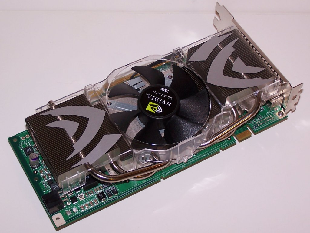
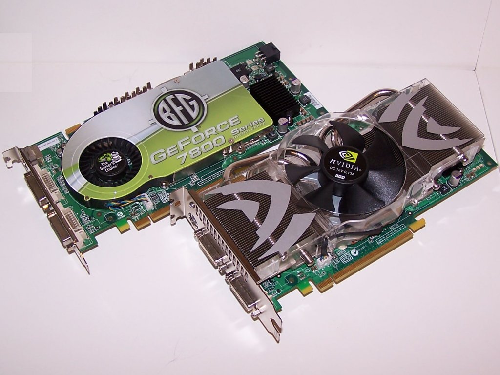
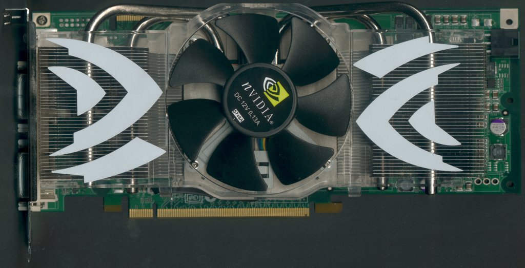
The most notable difference with the new 512MB board is obviously the cooling solution. The fact that NVIDIA used a single height cooler on the original GTX was an indication that there may still be more performance in the core, had it been cooled more aggressively, and that's the case with the new 512MB board, moving to a double height cooler solution. The cooling relies on a large fan in the centre of the board sucking air up and pushing it either side so that its partially vented out the back of the case and partially, internally, towards the front. Along the lines of the airflow are multiple small fins to increase the dissipation area, which are attached to the solid base which takes heat from the core and memory; heat is also moved away from the core up to the fins by the use of four heatpipes that start directly over the core, with two on each side moving around to the fins. This cooling solution is the same as that seen on NVIDIA's G70 based Quadro variant and can also be found on Leadtek's "WinFast PX7800 GTX TDH MyVIVO Extreme" - we've taken a closer look at the cooling here.
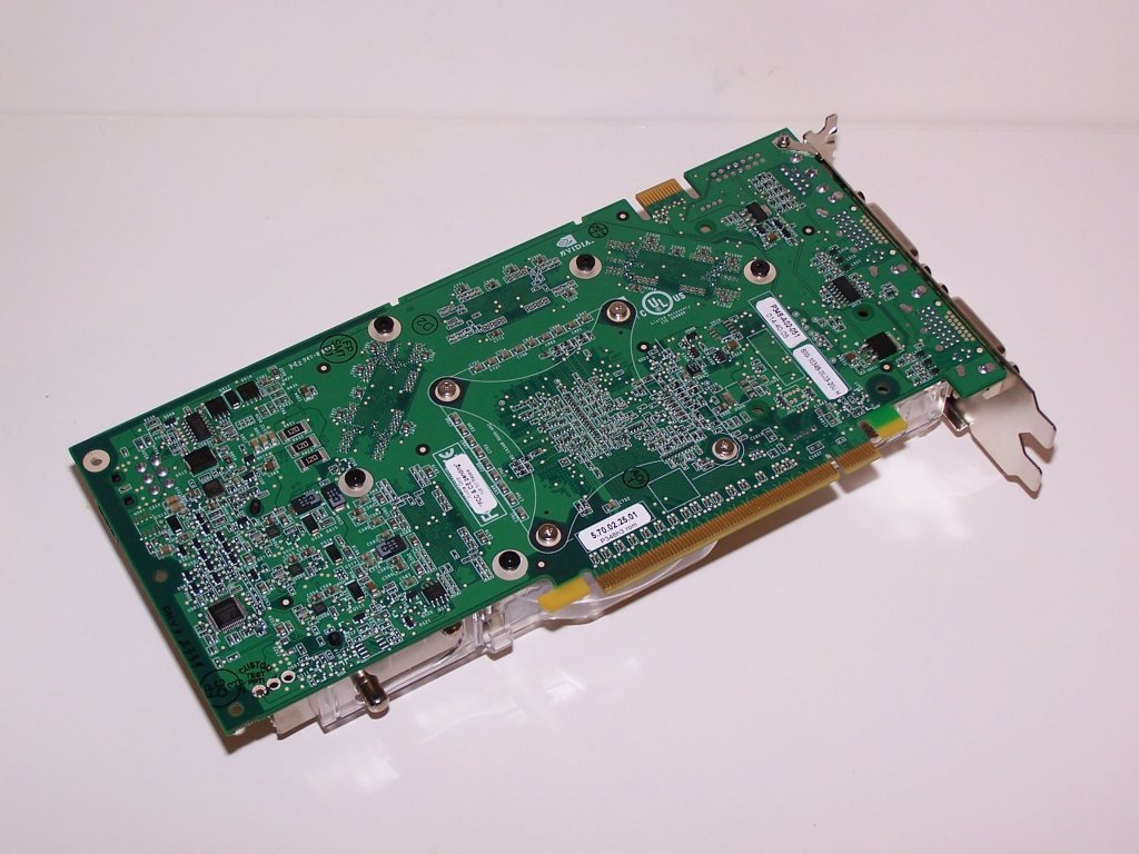
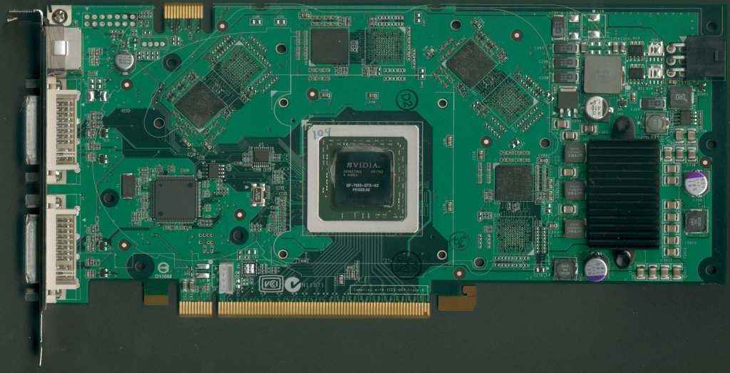
The board design for the new 512MB GTX has stayed largely the same as the previous 256MB board, however NVIDIA have needed to make some modifications to accommodate the new RAM chips. The memory used is Samsungs K4J52324QC GDDR3 memory rated at 1.1ns (a maximum of 900MHz). The layout of the 256MB GTX clearly indicates that NVIDIA had a 512MB capacity with 8 256Mb chips distributed across the front and back, but the blank spaces on the opposite side of the PCB to each memory chip could have been populated to double the capacity per channel; the memory chips used on the new 512MB GTX are of 512Mb density per module, meaning that 8 chips still only need be used to achieve 512MB, but also use the 136 ball packages, fewer than the memory chips used on the previous GTX, so the board has changed to accommodate that. Visibly there appears to be few other changes, except for the fan connector orientation and some extra power regulation components needed to cope with the increased power draw the higher clocked core and memory requires (although its interesting to note that the extra components used here were already provided for on the older board). The board I/O of this reference model is the same as that of previous GTX, with Dual DVI, one of which is a Dual-Link while the secondary is single, and a Video-In / Video-Out port for driving TV/HDTV displays and allowing video-input sources. It is likely that board vendors will stick with a similar output configuration as this.
|
|||||||||||||||||||||||||||||||||||||||||||
- NVIDIA Fermi GPU and Architecture Analysis
- ATI Cypress Gaming Performance Analysis
- ATI Cypress GPU and Architecture analysis
- ATI RV740 GPU and Architecture Analysis
- NVIDIA GT200 GPU and Architecture Analysis
- Dave Kirk - NVIDIA Tesla Launch
- Andy Keane Interview & Tesla Adoption/Deployment
- Diving into Anti-Aliasing
- Ian Buck - NVIDIA Tesla Launch
- Q&A with Visceral's Technical Art Director Doug Brooks on Dead Space 2
- AMD's John Bridgman on Radeon, Linux and Open Source 3D
- Travelling in Style: Beyond3D's C++ AMP contest - WINNER ANNOUNCED
- A speculative look on the Wii U GPU
- E3 2011: Behind Closed Doors - Witcher 2 Xbox 360... and a Nurse
- Was Harry Potter actually into rendering? Beyond3D's first ever book review
NVIDIA GeForce 7800 GTX 512MB Review - Page 2
Published on 14th Nov 2005, written by Dave Baumann for Consumer Graphics - Last updated: 29th Jul 2007
Page Navigation
Site width adjust
![]()
![]()
Reset width
Privacy Policy