The Chip - R600
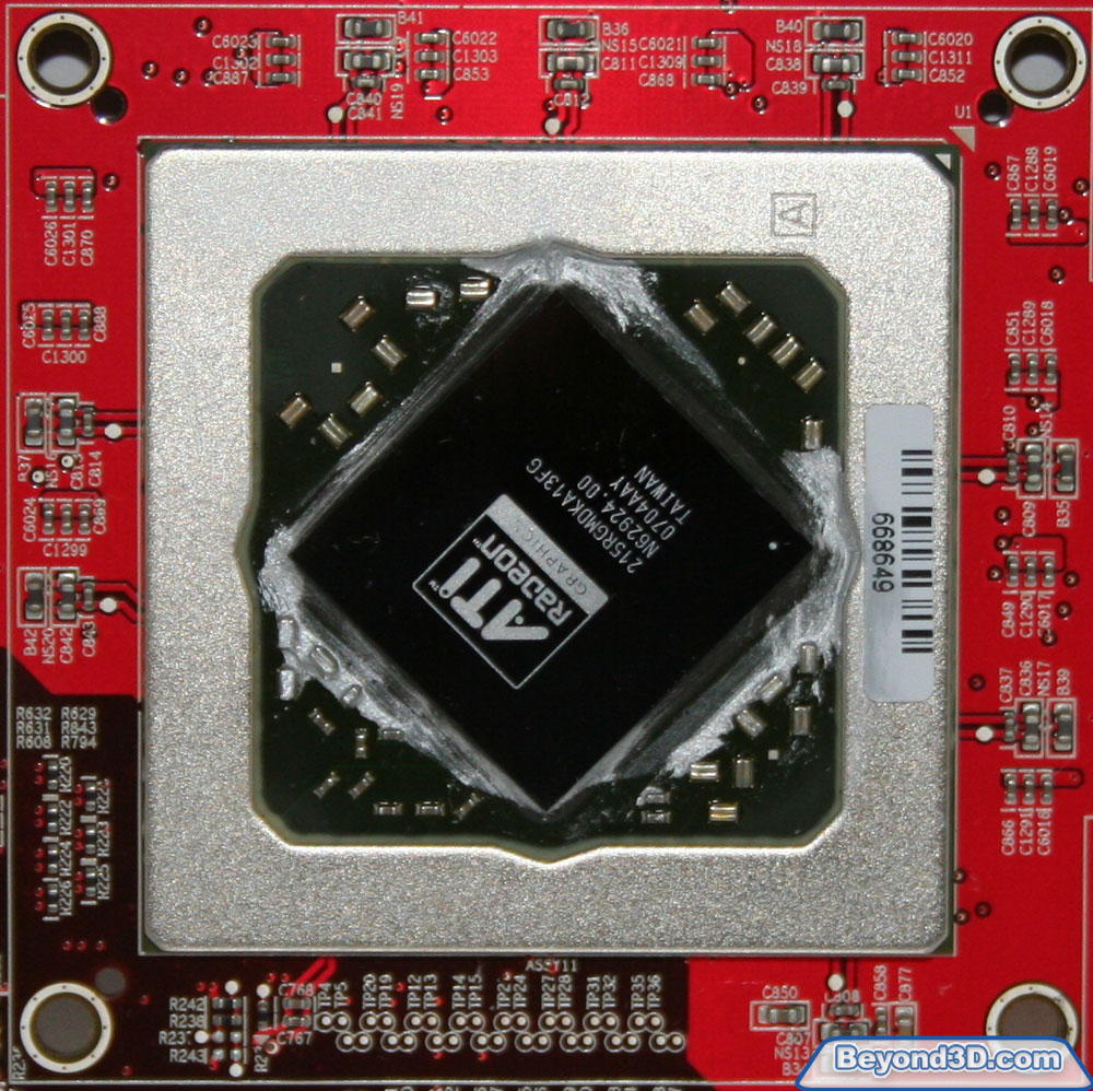
R600 is the father of the family, outgunning G80 as the biggest piece of mass market PC silicon ever created, in terms of its transistor count. It's not feature identical to the other variations, either, so we'll cover the differences as we get to them.
TSMC are AMD's foundry partner for this round of graphics processors once again, with R600 built on their 80HS node at 80nm. 720M transistors comprise the huge 20x21mm die, which contains all of the logic, including display and signal I/O. R600 is an implementation of AMD's 2nd generation unified shading architecture, fully threaded for computation, data sampling and filtering, and supporting Shader Model 4.0 as set out by Direct3D 10. R600 also sports a hardware tesselation unit for programmable surface subdivision and certain high order surfaces outside of any major existing API, although programmable using them.
R600 sports a 512-bit external memory bus, interfacing with an internal, bi-directional 1024-bit ring bus memory controller, with support for dozens of internal memory clients and GDDR3 or GDDR4 memories for the external store. Sticking with memory, the R600 architecture is cache-heavy internally, SRAM logic a significant portion of the die area. The external bus interface to the PC host is PCI Express, access to that coming via dedicated stop on the internal rings.
In terms of power management, the chip supports clock throttling, voltage adjust for p-states and entire unit shutdown depending on workload, combined by marketing under the umbrella of PowerPlay 7.
We'll cover all of those things and more as the article(s) progress. The initial R600-based SKU is called Radeon HD 2900 XT, so we'll take a look at the reference board before we move on to the architecture discussion for the chip that powers it. We'll cover RV610 and RV630 separately later today, as mentioned.