Memory Architecture
Although R420 had an upgraded, programmable memory controller in relation to R300, its design still stuck to many of the principles seen in ATI's earlier designs, however ATI felt that this standard, 4 way crossbar memory interface was running out of headroom from an implementation standpoint and from a performance standpoint. When chips start getting to the transistor numbers of R520 the relative size of the memory bus lengths begin to get rather large and costly, and the wires around the central controller start to get very dense, increasing the chances for hot spots on the chip and limiting the clock potential. To alleviate issues such as these ATI have done away with the old memory design and implemented an entirely new one.
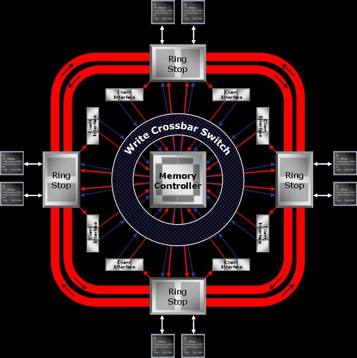
Ring Bus Memory Controller
As the diagram above illustrates the memory controller consists of the central controller, or arbiter, with the memory clients surrounding it that can make their data requests to the arbiter. All around the edges of the chip are two 256-bit ring busses, running at same speeds as the DRAM's, which run in opposite directions to reduce latency (dependant on where the data is going to or from it should only have to traverse a maximum of half the ring); by placing the memory bus around the edges of the chip wire density around the controller is decreased, which can result in higher clock speeds. There are 4 primary sequencer "Ring Stops" on the ring, where the data effectively gets on or off the bus, and on each of these ring stops are a pair of DRAM channels so that the ring bus is linked directly to the memory interface.
This is the flow of a client requesting some data (click the description for a pictorial representation):
- A client makes a request to the arbiter.
- The arbiter prioritises the request and, when ready, sends the request to a sequencer at the ring stop of the DRAM that houses the data.
- The data is retrieved from the DRAM, then traverses the ring until it gets to the closest ring stop to the original requester client.
Although only four ring stops are represented here, there is actually a smaller (1/16 the size of the others) fifth stop for other memory requests, inclusive of the PCI Express interface and the Video Input port.
The central controller is a programmable arbitration device, that can cater for multiple parameters. For instance, each of the clients will have different types of priorities and demands and each of the DRAM's will have different activities occurring on them, as well as the DRAM's own attributes dependant on the type of memory being utilised by the boards - the arbiter can take all of these different parameters into account and tries to prioritise the activities; for instance even if a client is usually of high priority but it its access type does not suit the exact activity occurring on the DRAM channel at that time it could allow other requests to be met if they will fit in with the current activity. The arbiter does have its own logic that constantly assess the activity and tries to tune itself to the demands that are going on in that session, however all the parameters are software updateable allowing for easy tuning of the memory bus via driver updates, and should ATI find an application that has requests that are abnormal in comparison to other applications could even set up individual application profiles to tune the memory interface specifically for that application.
Beyond just the addition of the arbitration login, ATI are claiming a 4x efficiency in random access of the memory by virtue of the fact there are now 8 memory banks per DRAM on the R520 memory controller, as opposed to 4 banks per DRAM on R420, and also 8x32-bit memory channels rather than 4x64-bit channels. To get the maximum efficiency out of the memory bus the memory channels should ideally carry enough data to max out the width of the channel and the burst length of the DRAM module - the wider the memory channel the less likely this is to occur, so breaking down the memory channel into even smaller width can increase the effective bandwidth utilisation. Up until now all 256-bit memory busses have utilised 4 way crossbar's, breaking the channels down to 4x64-bit busses; its likely that previous designs were not able to go down any further due to the trace density issues mentioned before - the ring bus mechanism now allows this to occur and also reduces the trace density, increasing the clock speeds. Note: the 8x32-bit channels is why we see an odd memory layout on the R520 boards, with one memory chip at angles to the top of the chip; normally 64-bit busses would need to have 32-bit chips paired together.
Although RV530 is a considerably smaller chip than R520, and only contains a 128-bit interface it does still utilise the same ring bus design, but in this instance uses two 128-bit internal busses. RV515 is too small to house such a memory controller, so defaults to more traditional crossbar design, although this time features 4x32-bit channels, which is the first time ATI have done this.
R520's memory controller already has the capabilities to support all current GDDR memory types, as well as GDDR4 which is coming in the near future. The design of the memory is such that it should scale to beyond 1.8GHz memory speeds over the course of its lifetime, which means that this memory design is likely to remain in ATI's designed for a few generations now; speeds in the order of 1.0GHz have already been achieved on R520.