The Shader Core
Just like Peter Parker, the RV740 has what can be regarded as great power in its shader core, provided by the sea of ALUs contained herein and the rather gobsmackingly high FLOPs/second they can produce in theory. However, just like in Peter Parker's case, a big back-breaking chunk of responsibility tags along with this great power and was placed straight on the shader compiler's lap -- you'll soon see why.
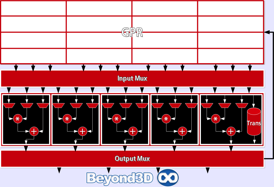
As you've already seen, ATI included 8 SIMDs (or clusters if you're thinking about other architectures and want a common parlance, outside of ATI's insistence on the SIMD nomenclature) in RV740, exactly twice as many as R600/RV670 had before it. Each SIMD consists of 16 blocks of 5 ALUs and 1 Branch Processing unit, organised in quads, for a grand and glorious total of 80 ALUs per SIMD and 640 ALUs per RV740. In theory, 5 instructions can be co-issued per cycle SIMD, assuming that the per-object instruction level parallelism required to do so is there.
Data dependencies conspire against achieving this maximum, however, and in a worst case scenario constituted by a sequence of fully dependent instructions, RV740 will run at around one 5th of its theoretical rate. However, keep in mind though that just like the first ideal case, this pathologically bad one is unlikely to be ubiquitous in real workloads. What can be said is that life is definitely interesting and challenging for Norm Rubin (ATI's lead compiler architect) and his team, because the compiler must do quite a bit of hoop jumping in its quest for extracting maximum ILP.
The structure of a packed VLIW passed for execution by a discrete block is made up of between 1 and 5 64-bit scalar ALU operations and at most 2 64-bit literal constants for a grand total of 7 64-bit words length. Control flow instructions are passed as separate 64-bit words assigned to the branch hardware. The 4 equal ALUs can handle 1 FP MAD/ADD/MUL/dot product per clock, or 1 INT ADD/AND/CMP/LSH*_INT (but not MUL!) per clock, to list just a few instructions.
For single precision floats, MUL and ADD are ½ ulp IEEE using round-to-nearest-even rounding, and MAD is 1 ULP with the same rounding mode. For double precision, as already mentioned, these ALUs are fused in pairs of two to compute 1 DP MAD per cycle across all 4 of them. Only a limited set of instructions are supported in DP (no transcendentals being the obvious omission), and compliance with IEEE754 is relative: denorms are flushed to 0, only round-to-nearest rounding is supported, and a MAD produces different results from MUL+ADD due to rounding. Integer and float instructions can't be processed in parallel.
The transcendental unit (the Rys unit!) is different from its more silhouette conscious brethren: it's (surprisingly!!!) capable of handling transcendentals (cos, sin, log, exp, rcp et al.) at a rate of 1/cycle, INT MUL, due to a slightly higher internal precision (40-bit versus 32-bit, allowing expression of a 32-bit int in the FP exponent) than the other ALUs, and format conversions, all whilst not being able to process dot products or double precision work (so it's idle when double precision processing is happening).
Up to now, the single differences from the RV670 reside in the integer bit-shifting abilities the normal ALUs have gained (before only the T/Rys-unit could do integer shifts). Work-assignment for the ALUs is also asymmetrical, the slim ALUs being tasked first, with the T ALU being the last to be issued an instruction, except when the instruction group contains transcendental or other instructions only it can execute, in which case it is immediately issued the corresponding instruction.
The fastest memory pool accessible to a SIMD is represented by the general purpose register file, which is even more lavish on the RV740, in spite of the fact that the R600/RV670 already had an ample supply. To be precise, we're talking about 2 MB in total, split equally amongst SIMDs. Within a SIMD, each block has a dedicated chunk within the register file section, to which it has exclusive access (this subset being arranged as a 4x256 matrix). In a single clock, any instruction can read from at most 3 distinct GPR addresses due to read port restrictions. The transcendental ALU shares GPR read ports with the other ALUs, so it can either load a needed operand in a single cycle if and only if one of the slim ALUs loads the same operand, otherwise it has to wait until such a time when an unused read port is available.
It's now time to talk about two innovations that R7 generation hardware, and by extension RV740, has introduced: the local data share (LDS) and global data share (GDS). We'll start with the GDS since it's considerably easier to tackle: it's the old memory read/write cache with a new catchier name and up-scaled capabilities and different accessing modes to match the architectural overhaul – or at least that's our very very very strong hunch, based on what we know of it. The GDS is a 16 KiB fully associative cache that is accessible to all SIMDs, thus allowing inter-SIMD communication. It's probable that GPRs are virtualised via the GDS, and that it's also useful for bypassing shader export and the ROPs to output directly to memory. It's important to note that for all intents and purposes the GDS is opaque to software, being impossible to interact with it programatically -- another reason to look at it as a mild evolution of the old R/W cache, serving a very specific purpose.
Moving to the LDS though, it's definitely a completely new thing that wasn't present in R6 chips. As you've noted, each SIMD gets its own 16 KiB LDS, which is arranged in 4 banks, each bank containing 256 16-byte entries. It's a purely compute-oriented affair, its purpose being to allow for low(er)-latency data-sharing between multiple compute threads assigned to the same SIMD, as well as within them. Writes are owner-exclusive (only the owner thread can write to the owned location), reads are shared (all other threads can read any location). We've not toyed with the LDS enough to go into more details, but that will happen sooner rather than later (hopefully ATI makes its documentation a bit more clear as well).
Putting all of the above together, it's pretty obvious that the RV740, in spite of being value oriented chip, can produce some serious number crunching when the compiler gods smile at it and the instruction streams flow as if arranged by Richard Huddy himself. In the real world, it is significantly more challenging to taste those 1.2Top/s peak, be it in graphics workloads or in general compute ones. Finally, irrespective of how the compute per bit ratio grows, sooner or later you will have to feed the shader core via the samplers, and even the most adept math-cruncher can be hamstrung by insufficient sampling capability (not to mention that typical workloads also like to do nasty things like filtering). Knowing that this has been a sore-spot in the past for ATI, looking at how sampling is handled in RV740 should prove most interesting.