Cypress High-level View
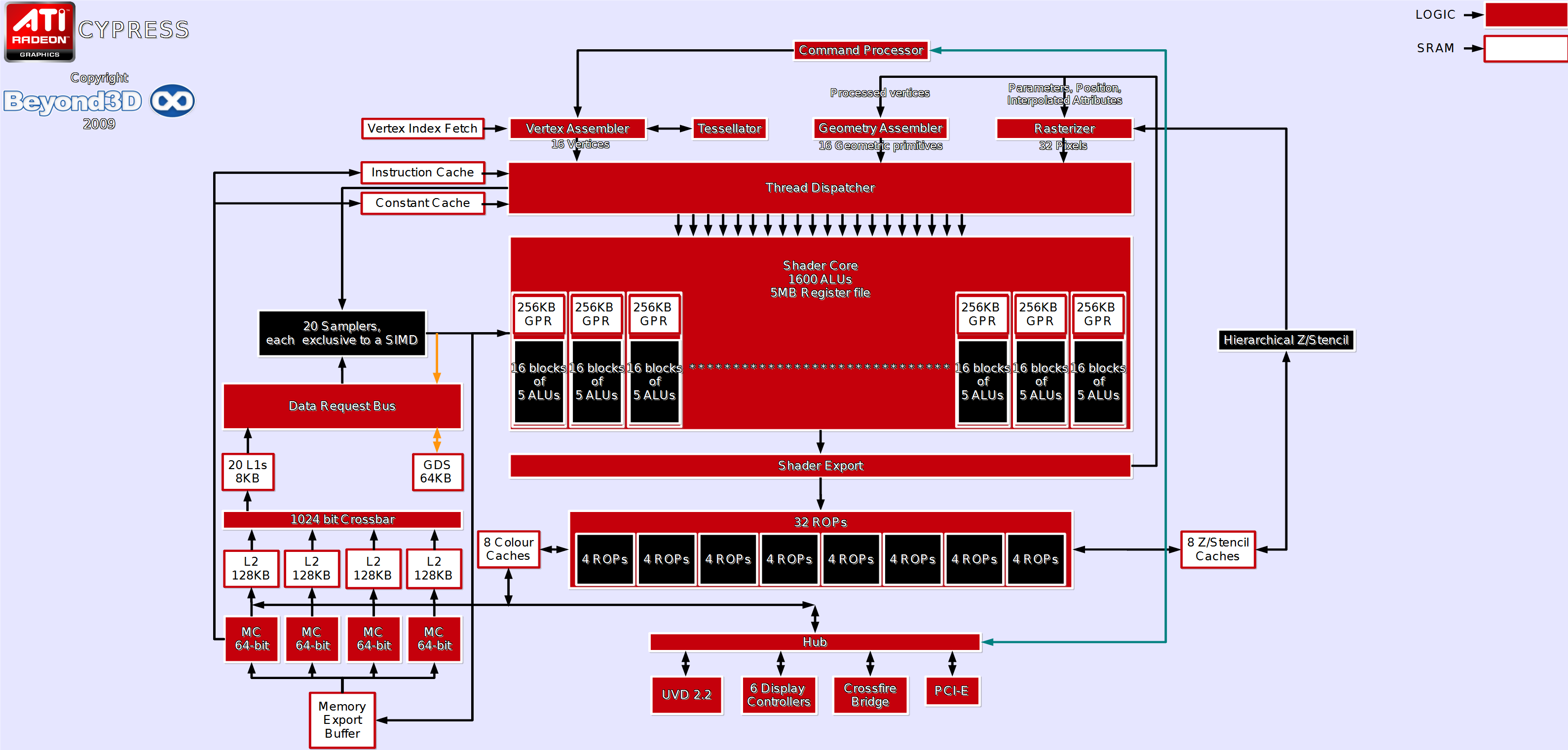
What you have above is a rather simplified overview of how Cypress is laid out. It's by no means exhaustive, but it should definitely give a general idea about how things work. You can notice the doubling happening on multiple levels versus the RV770, whilst also taking into account that the basic tenets of the architecture haven't changed all that much. The shader core is still split into 80 ALU SIMDs comprised of 16 blocks of 5 ALUs. The ALUs are capable of both single and double precision processing, also claiming IEEE754-2008 compliance. They're also asymmetrical just like before, with 4 slim ones and the 5th T/Rys unit. However, the slim guys have learned some new tricks and many non apparent tweaks have been implemented, so it's not just a simple case of multiply by 2 and forget about it.
The tessellator, an old acquaintance, moves to the role of first class citizen under DX11, with expanded capabilities, although we have a rather strong hunch that at the constructive level the hardware is quite similar to what was present before. You may want to keep the diagram open in a separate window for referencing as we proceed to detailing every functional aspect.