The Shader Core

Entered the temple of FLOPs, we have...and they are legion! 1600 ALUs conspiring to provide a maximum theoretical math-crunching rate of 2.72 TFLOPs/s are definitely something noteworthy. However, getting to see those FLOPs in practice is a somewhat hairy affair.
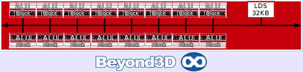
The general organization we first encountered way back in the day with the R600 is still here: SIMDs made up of 16 blocks of 5 ALUs, depending on exploitable ILP in the instruction stream. There are 20 such SIMDs, and physical arrangement of the shader core has changed versus the RV770, with SIMDs being split in two 10 tall blocks symmetrically placed versus the central data request bus. Mind you, this is a physical layout change, logically they work in pretty much the same way, with a similar flow.
As you've probably already deduced, assuming sufficient ILP exists, and the compiler works its magic, up to 5 instructions can be co-issued per ALU block. However, dependencies can reduce it to as little as 1 instruction per cycle, in a purely serial instruction stream. From what we've seen, the general case seems to be around 3-4 instructions packed per cycle, which is decent. Speaking of packing, that's how the ALU blocks get their instructions, in a packed VLIW that can contain anywhere between 1 and 5 64-bit scalar ALU ops (lots of bits there, which gives you an idea about the complexity of this GPU's ISA), and up to two 64-bit literal constants. Control flow instructions are separately dispatched as 64-bit words, for execution on the branch processing unit.
The 4 slim ALUs handle all of their old tricks, so each is capable of 1 FP MAD/ADD/MUL or 1 INT ADD/AND/CMP, as well as integer shifts. Cypress adds to its slim ALUs the capability to do single cycle 24-bit INT MUL whereas before no INT MUL support existed at all. Getting the 24-bit INT is fairly easy, since the slim ALUs are FP32 so there are enough mantissa bits there to represent it, but there's not enough for a full 32-bit INT. There's also FMA support, which will bring benefits versus a simple MAD when it comes to precision loss introduced by rounding involved in the latter.
Moving to the artist formerly known as the RysUnit, currently known as the transcendental ALU after it threatened to sue, it remains a rather special chap, being higher precision than the other units (FP40 versus FP32). It can handle transcendentals, just like before, each being single cycle at least according to our measurements. It can also do a single 32-bit INT MUL per cycle, by virtue of it's more accommodating mantissa with a noteworthy difference being that it can't do FMA.
Scheduling within the ALU block follows a certain set of rules: if the instruction mix contains instructions that can be executed across all ALUs, the slim ALUs are the ones that first get issued instructions, with the transcendental ALU being last, if there are instructions left to issue. If an instruction that can be executed only on the transcendental unit is present, it's obviously immediately issued to it. These restrictions are tied into how the GPR file is organized and how read/write access is laid out. Each ALU block has exclusive access to 1024 128bit GPRs arranged as a 4x256 matrix and the maximum number of GPR addresses that an instruction can reference is 3. We're almost certain that the transcendental ALU still shares read/write ports with the slim ALUs – considering that SRAM scales in size with roughly the square of the read/write port count, adding 3 extra ports would've been pretty costly – which means that it's ability to fetch operands from GPRs is somewhat restricted.
It can perform a single cycle fetch (the other ALUs can't), only if one of the slim ALUs needs and fetches the same operand. Otherwise, it must wait for a cycle in which read ports are available. This is one of the reasons for which even for instruction mixes that are comprised of wholly independent instructions, you can at times not achieve maximum ALU throughput. Now you see that one of the goals of the scheduling rules within an ALU block is to minimize GPR access contention. Doing a wee bit of math here again, you've probably already determined that Cypress has a total register file of ~5.12MB which in and of itself is almost as much SRAM as one could find on an RV770 in total.
And all of this register file talk brings us to another Cypress innovation, namely something that ATI vaguely dubbed single clock co-issuing of a MUL and a dependent ADD. Actually, this is a tweak aimed at reducing register file pressure, by leveraging the pipelined nature of the ALUs: the result of the MUL is latched, instead of being written back into the registers, so both a write as well as a read are saved, however, this does not directly increase instruction issue rate and it also does not mean that the pair gets fused.
In the vein of tweaks, it's time to do a bit of educated speculation about another such element implemented in Cypress, but one that we have not yet had the time to check, namely dot products with more flexibility than plastic man's! Our guess is that this means that for a DOTn, where n<4, the instruction will no longer be handled as a DOT4 with components masked, which was the case for prior architectures and which translated into inefficient usage of the ALUs, but rather a proper DOTn will be issued using only as many ALUs as necessary and freeing others for other instructions.
Borrowing a page straight out of the CPU designer's manual, where adding instructions with extremely specific applicability, there's also a new SAD (whether it's better to be MAD or SAD is up to anyone's guess) instruction, which is almost certainly implemented via microcode. It'll probably be useful for video encoding or image processing, but it falls outside of API boundaries and will only be available as an OCL extension or to driver internals.
Double-precision math is still present, done in pretty much the same fashion introduced by the RV670: the slim ALUs gang-up in pairs of two, one working on the high bits and the other working on the low bits of a 64-bit value. This translates into the ability to do 2 DP ADDs, 1 DP MULs or 1 DP MAD/FMAD per cycle. Transcendentals are still no-go for DP, but compliance with IEEE754 is more complete now, with de-norms being properly signalled (they were flushed to 0 before), alongside NaNs or Infs.
However, overflow and underflow support is still incomplete, in that whilst the occurrence of one or the other is properly signalled, one cannot implement a catch routine to handle them in code. Since simply crashing would be quite bad, we assume that an over or underflow results in either getting a 0 or a NaN carried through the computation, most likely a 0.
In order to match DX11 requirements, ATI had to double the size of its Local Data Share, from 16 KB to 32KB, whilst also implementing a more flexible access model: whereas before a restrictive read global/write private policy was in place, with thread count conditioning per-thread LDS write-space availability, in Cypress the LDS is read global/write global, with threads having access to the full LDS for writes if needed irrespective of total thread count. This obviously applies to threads belonging to the same group executing on the same SIMD, since the LDS is aimed at providing low latency data-sharing for these. What's unclear is whether or not LDS bandwidth has been expanded versus the RV770, since this was a potentially limiting factor. By the time we had setup things to measure it, we had already been separated from the hardware so that mystery will remain unravelled for a little more time.
For data sharing between threads that are part of separate groups matched to separate SIMDs, there's the Global Data Share, which has also been expanded to 64KB. However, we can't say more about it since it's a rather opaque chunk of SRAM at this point in time: there's no way to access it in code, and ATI has been anything but verbose on the topic. We're told that an OpenCL extension will expose it, and that currently it's up to the compiler to figure out how to best use it, which to be honest isn't necessarily confidence inspiring. A significant overhaul with regards to inter-SIMD interaction is the inclusion of Global Synchronization Registers, which means that now you can implement a synchronization primitive like a semaphore on a global level, synchronizing execution across all SIMDs. This was not possible in the RV770 or prior ATI parts, at least as far as we're aware.
The ALUs can bypass the ROPs and stream-out data directly to memory via the Memory Export Buffer. Its size is 256B, twice as large of what could be found in the RV770, and you can deduce from its size that up to 64 32-bit words can be written per cycle. Speaking about exports, we've measured an improvement in export rates, something in the area of 30% at most, with some in-house shaders we have that were export limited on the RV770/790.
Overall, the situation with the shader core is similar to all prior AMD architectures in recent memory: there's a huge amount of potential performance available, but getting it can potentially be challenging. It's definitely gained some flexibility versus something like the RV770, but also some new pitfalls – we're looking at you here, computed-on-ALUs attribute interpolation, and your impact on scheduling complexity and register pressure. We do think that by this point in time ATI's compiler is quite apt at handling graphics, and we expect to see rather impressive ALU utilisation rates there, except in cases where “poisoned” code is involved, but it remains to be seen how things pan out in the newly emerging area of GPU compute, where depending on how adventurous one is, register pressure and scheduling hazards are more likely to manifest themselves. Another significant member of the GPU performance equation is data sampling, because a sea of ALUs that can't be fed data to work on is not that useful, so time to see what happened on that front.