Xbox 360 System Overview
The "XBOX 360" console was officially unveiled at a show on MTV the week prior to E3 2005, and at the unveiling Microsoft revealed a few technical details of the platform. The primary specifications for the system are:- 3.2GHz Custom IBM Central Processor
- Three CPU Cores
- Two Threads Per core
- VMX Unit Per Core
- 128 VMX Registers Per Thread
- 1MB L2 Cache (Lockable by Graphics Processor)
- 500MHz Custom ATI Graphics Processor
- Unified Shader Core
- 48 ALU’s for Vertex or Pixel Shader processing
- 16 Filtered & 16 Unfiltered Texture samples per clock
- 10MB eDRAM Framebuffer
- 512MB System RAM
- Unified Memory Architecture (UMA)
- 128-bit interface
- 700MHz GDDR3 RAM
Of these core components obviously we are going to be most concerned with the graphics processing element. Whilst the graphics processor is different from others seen before in the PC space, and is very different from even ATI's impending new PC graphics components, it will be interesting to take a look at the graphics processor for the very reason that it doesn't directly correspond to any current graphics processor but also because we feel that this will give hints as to the architectural direction ATI are likely to be taking in the future for PC and other applications.
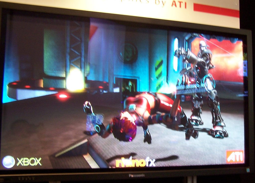
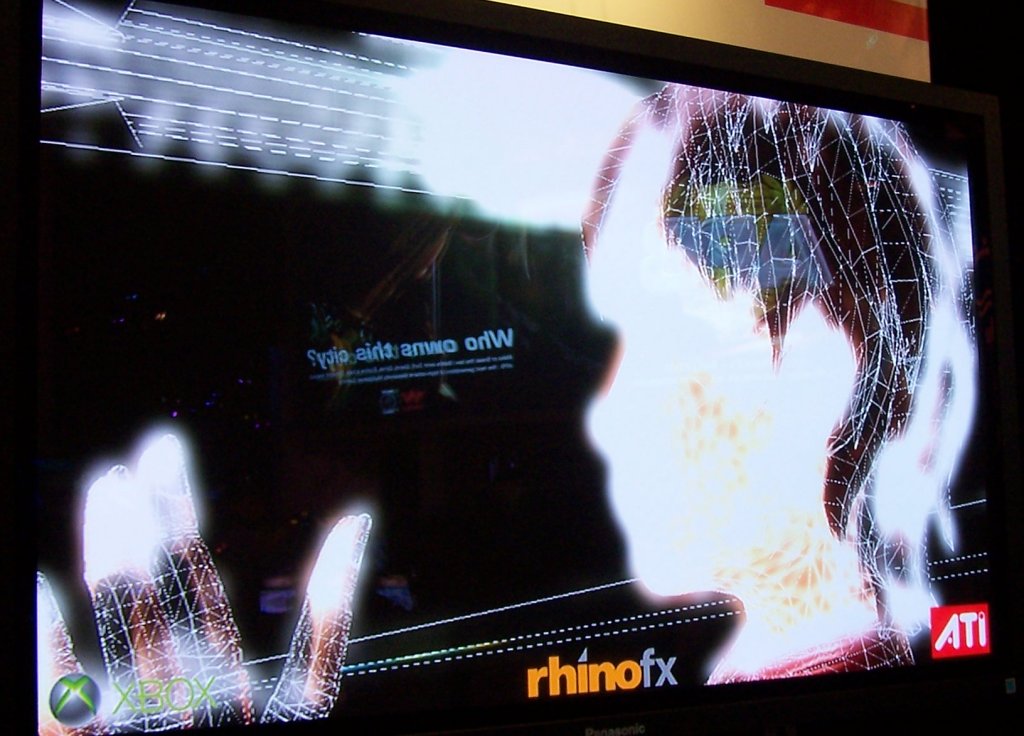
ATI C1 / Xenos
A name that has long since been mentioned in relation to the graphics behind Xenon (the development name for XBOX 360) is R500. Although this name has appeared from various sources, the actual development name ATI uses for Xenon's graphics is "C1", whilst the more "PR friendly" codename that has surfaced is "Xenos". ATI are probably fairly keen not to use the R500 name as this draws parallels with their upcoming series of PC graphics processors starting with R520, however R520 and Xenos are very distinct parts. R520's aim is obviously designed to meet the needs of the PC space and have Shader Model 3.0 capabilities as this is currently the highest DirectX API specification available on the PC, and as such these new parts still have their lineage derived from the R300 core, with discrete Vertex and Pixel Shaders; Xenos, on the other hand, is a custom design specifically built to address the needs and unique characteristics of the game console. ATI had a clean slate with which to design on and no specified API to target. These factors have led to the Unified Shader design, something which ATI have prototyped and tested prior to its eventual implementation ( with the rumoured R400 development ? ) , with capabilities that don't fall within any corresponding API specification. Whilst ostensibly Xenos has been hailed as a Shader Model 3.0 part, its capabilities don't fall directly inline with it and exceed it in some areas giving this more than a whiff of WGF2.0 (Windows Graphics Foundation 2.0 - the new name for DirectX Next / DirectX 10) about it.
The Xenos graphics processor is not a single element, but actually consists of two distinct elements: the graphics core (shader core) and the eDRAM module. The shader core is a 90nm chip manufactured by TSMC and is currently slated to run at 500MHz*, whilst the eDRAM module is another 90nm chip, manufactured by NEC and runs at 500MHz* as well. These two chips both exist side by side, together on a single package, ensuring a fast interlink between the two. The main graphics chip, the parent core, could be considered as a "shader core" as this is one of its primary tasks. The eDRAM module is a separate, daughter chip which contains the elements for reading and writing color, z and stencil and performing all of the alpha blending and z and stencil ops, including the FSAA logic. We'll explore the capabilities and operations of both these chips in greater detail throughout the article.
(*) Note: We understand the clockspeeds for the shader core and daughter die are target clockspeeds at present and there may be some room for small movement either way on both dies dependant on yields. As Microsoft have now announced 500MHz speeds it is more likely that these will be the eventual release speeds.
One element that has been reported on is the number of 150M transistors in relation to the graphics processing elements of Xenon, however according to ATI this is not correct as the shader core itself is comprised from in the order of 232M transistors. It may be that the 150M transistor figure pertains only to the eDRAM module as with 10MB of DRAM, requiring one transistor per bit, 80M transistors will be dedicated to just the memory; when we add the memory control logic, Render Output Controllers (ROP's) and FSAA logic on top of that it may be conceivable to see an extra 70M transistors of logic in the eDRAM module.
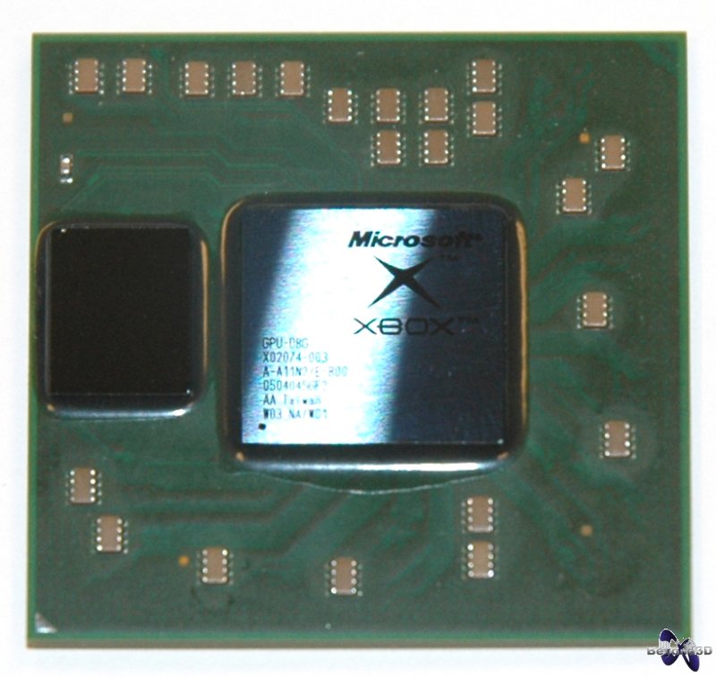
Update: We've recently been given an image of the Xenos graphics chip package (above) that highlights the dual die nature, with the parent die quite clearly to the centre of the package and the daughter over to the left. While the 232M transistor figure for the parent was given to us by ATI we are still trying to establish a more official figure for the daughter (even though these types of transistor counts are very much estimates anyway). We've speculated that the 150M figure that appeared when XBOX 360 was first announced may just relate to daughter die, however another figure that has arisen is 100M - judging from the die sizes the daughter die doesn’t have more than half the area of the parent, which would giv indications towards the 100M side although 80M of those transistors are DRAM which may be more dense than the logic circuitry that will dominate the parent die. We are trying to get further clarification.
One of the mistakes that Microsoft made with the original XBox was to contract their component providers into supplying entire chips with, evidently, no development path - at least, this was the case with NVIDIA NV2A graphics processor, which resulted in Microsoft and NVIDIA going through a legal arbitration process. Although the components in the XBOX 360 in its initial form are hardly low cost, the cost of the unit over the course of its lifetime is one that has quite obviously been addressed with contracts that pay via royalties for chips sold and with Microsoft in charge of ordering the chips from the various Fabs, however the original semiconductor manufacturers are likely to still be in charge of further developments in terms of putting the cores on to smaller processes and we believe that this is part of the contract that ATI has with Microsoft. An obvious area for cost reduction of the Xenos processor is by merging the shader and daughter die on to a single core - we suspect that this will not happen until there is a process shrink available (that can also cater for both the complex logic and eDRAM) as two cores on 90nm mitigate some of the yield risks of a single, large die on 90nm.