Bandwidths and Interconnects
When creating a high performance computing platform bandwidth between components and operations is highly important, especially when creating a system that has to last for 3-5 years before a new version comes about, such is the world of consoles. With the Xenos processor being both a high performance graphics processing element of the XBOX 360 as well as the "Northbridge" component of the system, which is essentially the communication hub for the other components of the system, it has many interconnects and bandwidths to deal with. Below is a diagram highlighting the connection bandwidths between the most important elements it is connected to:
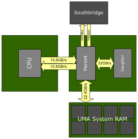
As we discussed earlier, the XBOX 360 carries a unified memory architecture and Xenos's parent die is acting as the Northbridge controller as well as the graphics processing device. The system memory bandwidth is 22.4GB/s courtesy of the 128-bit GDDR3 memory interface running at 700MHz. At 232M transistors the Xenos parent die isn't an enormous chip so internal memory communication isn't going to be too latency bound, hence the memory interface only needs to be a standard crossbar, which is partitioned into two 64-bit blocks. Xenos's parent die also has a 32GB/s connection to the daughter, eDRAM die Connection to the Southbridge audio and I/O controller is achieved via two PCI Express lanes which results in 500MB/s of both upstream and downstream bandwidth.
As the CPU is going to be using Xenos to handle all its memory transfers, the connection between the two has 10.8GB/s of bandwidth both upstream and downstream simultaneously. Additionally the Xenos graphics processor is able to directly lock the cache of the CPU in order to retrieve data directly from it without it having to go to system memory beforehand. The purpose of this is that one (or more, if wanted) of the three CPU cores could be generating very high levels of geometry that the developer doesn't want to, or can't, preserve in the memory footprints available on the system when in use. High-resolution dynamic geometry such as grass, leaves, hair, particles, water droplets and explosion effects are all examples of one type of scenario that the cache locking may be used in.
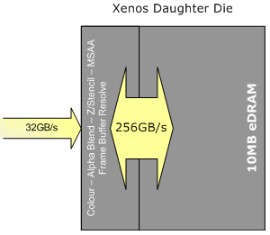
The one key area of bandwidth, that has caused a fair quantity of controversy in its inclusion of specifications, is that of bandwidth available from the ROPS to the eDRAM, which stands at 256GB/s. The eDRAM is always going to be the primary location for any of the bandwidth intensive frame buffer operations and so it is specifically designed to remove the frame buffer memory bandwidth bottleneck - additionally, Z and colour access patterns tend not to be particularly optimal for traditional DRAM controllers where they are frequent read/write penalties, so by placing all of these operations in the eDRAM daughter die, aside from the system calls, this leaves the system memory bus free for texture and vertex data fetches which are both read only and are therefore highly efficient. Of course, with 10MB of frame buffer space available this isn't sufficient to fit the entire frame buffer in with 4x FSAA enabled at High Definition resolutions and we'll cover how this is handled later in the article.
Both XBOX 360 and Playstation 3 feature UMA and graphics busses, respectively, that have been announced to use fairly fast 700MHz GDDR3 memory, but both only have a 128-bit interface. Whilst this is less of a surprise for XBOX 360 as Xenos's use of eDRAM will move the vast majority of the frame buffer bandwidth to the EDRAM interface leaving the system memory bandwidth available primarily for texturing bandwidth. It does seem odd that by the time the consoles will be released the likelihood is that high end PC graphics will using at least the same speed RAM but on double wide busses. The primary issue here is, again, one of cost - the lifetimes of a console will be much greater than that of PC graphics and process shrinks are used to reduce the costs of the internal components; 256-bit busses may actually prevent process shrinks beyond a certain level as with the number of pins required to support busses this width could quickly become pad limited as the die size is reduced. 128-bit busses result in far fewer pins than 256-bit busses, thus allowing the chip to shrink to smaller die sizes before becoming pad limited - by this point it is also likely that Xenos's daughter die will have been integrated into the shader core, further reducing the number of pins that are required.