NVIDIA G80 Overview
A
product of a mental technique used to gather my thoughts on previous
architecture analysis endeavours, the following diagram represents a
somewhat high-level look at how G80 is architected and what some of the
functional units are capable of. After the guts of a chip analysis is
complete, I find it helps to draw it out (usually on a huge sheet of
paper) to organise data flows, note down specs and rates and get a
picture of it mentally to refer to when describing the thing in text.
This time it turns out that the drawing is decent enough for public
consumption and as a basis for what we'll talk about. Click for the
full-on version, and be prepared for an altogether scarier one later
on.
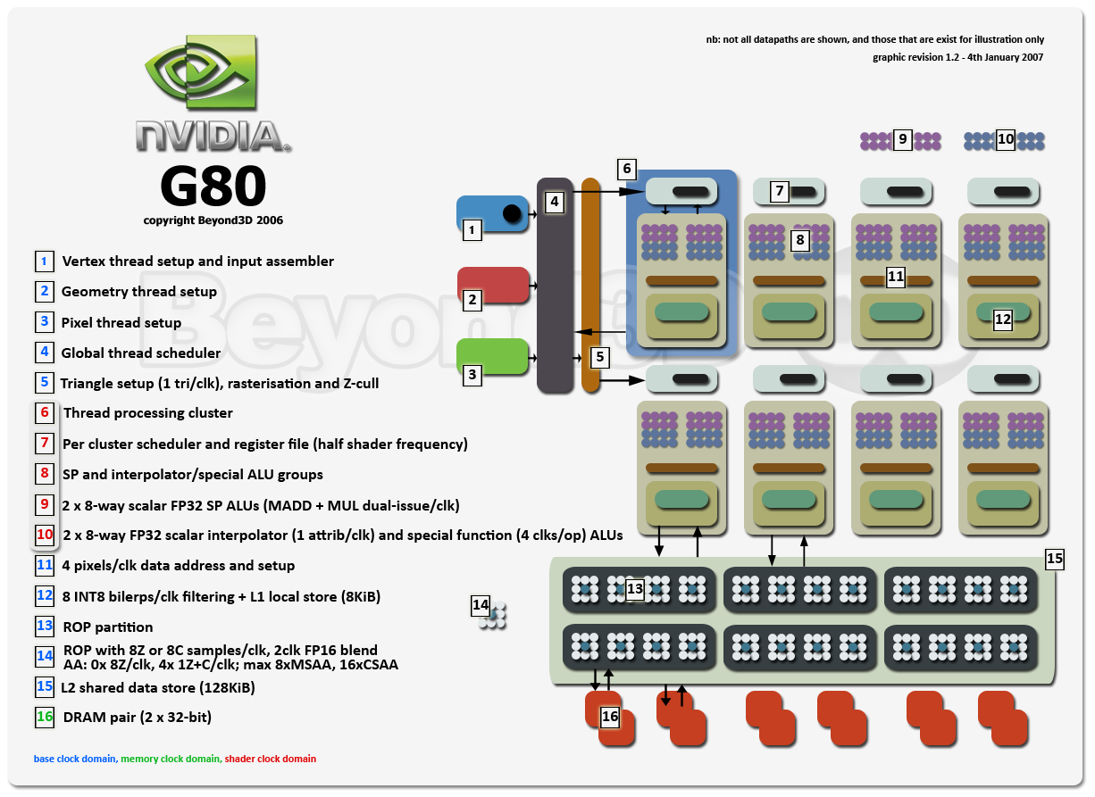
If it's not clear from the above diagram, G80 is a fully-unified, heavily-threaded, self load-balancing (full time, agnostic of API) shading architecture. It has decoupled and threaded data processing, allowing the hardware to fully realise the goal of hiding sampler latency by scheduling sampler threads independently of and asynchronously with shading threads. Its primary ALU structure is fully FP32 and completely meets IEEE754 standards for computation and rounding of single precision floats, and supports most '754 specials other than denorm signalling and propogation.
So let's start with the front end of the chip, following data flow pretty much from 1 to 16 on the diagram. We suggest you keep the diagram open as a reference as you progress through the article, to help make some of the text make a bit more sense.