Although this is the first time that Beyond3D has seen a GeForce FX-based board we won't go into an explanation of its features as we've covered much of that already. If you wish to know more about the features of the GeForce FX then see the following articles:
- ATI R300 & NVIDIA NV30 - A Technical Comparison
- NV30 Announced: GeForce FX
- GeForce FX Launch & Interview
- GeForce FX Tech Q&A
The Chip, The Board
Here's a quick recap of the chip / board technical specifications, as per NVIDIA:
| Specifications | |
| Chipset | NV30 |
| Silicon Process | .13µ (TSMC) |
| Transistor Count | ~125 Million |
| Engine Clock | 500MHz |
| Pixel Pipes x Texture units | 8x1 4000Mpixel/s / 4000Mtexels/s * |
| Memory | 128/256MB 1000MHz(500MHz DDR-II) 128-bit interface = 16GB/s Bandwidth |
| RAMDAC | Dual 400MHz |
| Bus Standard | AGP 8X/4X/2X |
* See the 'Theoretical Performance' tests, later in this article, for more on the fill-rate calculation
At a 125 Million transistors NV30 weighs in at nearly exactly double the complexity of their previous generation NV25 chip.
Here's a few images of the reference board:

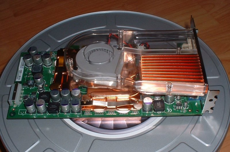
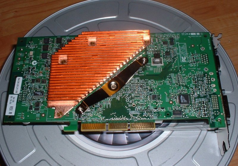


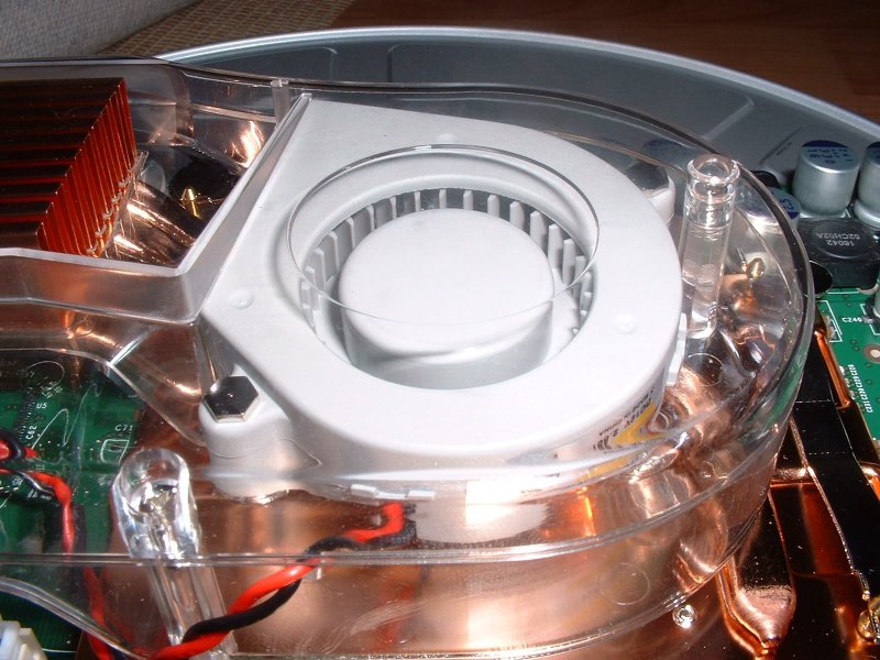
As we can see, this unit employs the 'FlowFX' cooling system that features plenty of copper heat-sinks, heat pipes and a ducted fan mechanism for cooling. This is a first revision .13µ board, and running at 500MHz it gets very hot, which is why this rather elaborate cooling mechanism is required. The 500MHz DDR-II RAM also runs hot which is why there are large hea-tsinks covering the RAM - you'll note that the underside of the board, which faces upwards when mounted in the AGP slot, has a heat-sink that generates a reasonable amount of heat directly under the CPU.
We've seen a few revisions of the 'FlowFX' cooling solution since the first previews of GeForce FX 5800 Ultra's were made available, and judging by the clear plastic ducting this would appear to be the later revision. This revision is supposed to run quieter in 3D mode than the previous versions, yet the fan noise is still quite loud and can be heard over my other PC's Lian-Li case, with 4 system fans and a CPU fan. This version does spin down entirely in 2D modes (which runs at 300/300), which means the board is passively cooled, and completely silent. During testing the fan did spin down quite frequently, presumably because the board was overheating, when running 3D applications, also reducing its 3D performance.