
What is CMOS photonics, and what does it actually replace? Imagine what happens when data leaves a chip: purely digital information (bits with a value of 0 or 1) is transformed into a modulation in the analog domain. In the case of wired interfaces, this modulation is traditionally electrical and will be transmitted through a copper interconnect either on-PCB or via an external cable. The part that performs this conversion on both ends of the connection is the transceiver, which is also sometimes called a physical layer or PHY. As it is fundamentally analogue, it does not scale with Moore's Law.
In addition to the PHY, you normally also have digital logic, of course. As a practical example, look at AMD's upcoming Barcelona. On RealWorldTech.com's die shot, you will notice that the DDR2 and HyperTransport PHYs are quite big... in fact, they're bigger than the integrated digital northbridge! Clearly, this could have been one of the factors that hurt scaling for the 65nm Brisbane, as PHYs don't shrink much if at all between process sizes. Also, notice that in this example we're just trying to push data from one chip to another; for a given bitrate, that's obviously much easier (and cheaper) than trying to do the same via an external cable. As an another example, if you look at integrated Ethernet on motherboards, the digital part (the MAC) is integrated on the southbridge but the PHY never is. It's a much better idea to manufacture that separately, as it is fairly large and does not scale with process generations.
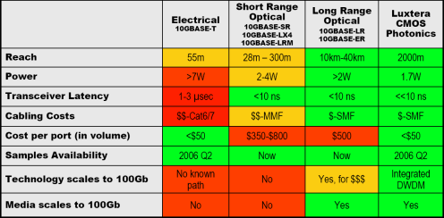
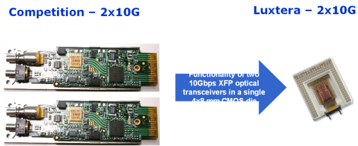
We mentioned earlier that copper cables are reaching their physical limits. However, traditional transceivers have problems of their own. Compared to their 1Gbit counterparts, 10Gbit Ethernet transceivers can be power hungry (<1W vs <15W) and much more expensive (<$5 vs <$50). Beyond 10Gbit, these problems would be so enormous that traditional transceivers and copper interconnects wouldn't even be viable options. At that point, you'd have to turn to optical systems with assembled parts and low yields, which means even higher costs. That's where Luxtera comes in.
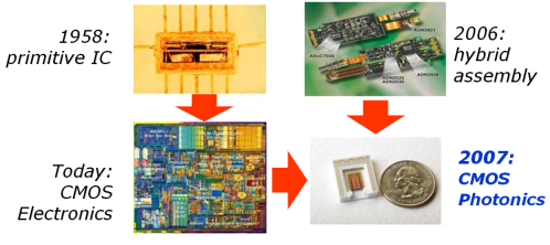
Without going into too much detail on how the technology works, we'll look at why this is possible today but wasn't 10 years ago. CMOS photonics is the idea of manufacturing optical functionality on a semiconductor chip, via either a fully standard or slightly modified semiconductor manufacturing process. In short, it combines traditional electronics and optics on the same die.
Luxtera, being a fabless start-up, is using a standard production line at Freescale, who also produces PowerPC CPUs. Intel, on the other hand, has the luxury of being able to use a custom process with exotic materials. Regardless, the growth of CMOS photonics seems to have primarily resulted from the following factors:
- The continuous scaling of semiconductor processes in the last decades, as suggested by Moore's Law, has resulted in the capability to cost-efficiently mass produce very large amounts of nanoscale structures that are actually smaller than the wavelength of visible light (400-750nm). Precision is good enough to manufacture optical functionality on the chip, including "waveguides." This is only possible because silicon is transparent to infrared light.
- SOI processes (silicon-on-insulator), as used by IBM, AMD and Freescale, among others, have another very attractive attribute for optics. The refractive indices of silicon and the silicon dioxide (SiO2) used as an insulator are very different. This allows for total reflection to occur, which can be used to control the light and make sure it remains in a specific area when needed. This could be done with materials other than SiO2, but then CMOS photonics would not be possible on a mainstream process.
- As we've mentioned several times, copper-based solutions are approaching their physical limits. Given copper's total dominance in these fields at the moment, that is really a major market opportunity that makes research even more appealing. Ten years ago, the financial prospects would likely have been much less attractive, so it's not very surprising things are only spicing up right now.
Luxtera's CEO himself has recently recognized this as a more elegant and simply better long-term approach, but not doing it that way allows Luxtera to have a significant time-to-market advantage while also bypassing the manufacturing issues of using a custom process. The company is hedging its bets by trying to have a similar technology ready in time to compete with Intel's custom solution, but it remains to be seen how and where that will be manufactured.
That's all well and good, but what do CMOS photonics and ultra-high-bandwidth interconnects have to do with HDMI, DisplayPort and you? What, you mean it isn't obvious yet?