S3
VIA’s graphics division, S3, are currently pushing their latest chip, S18 that powers the GammaChrome series of boards.
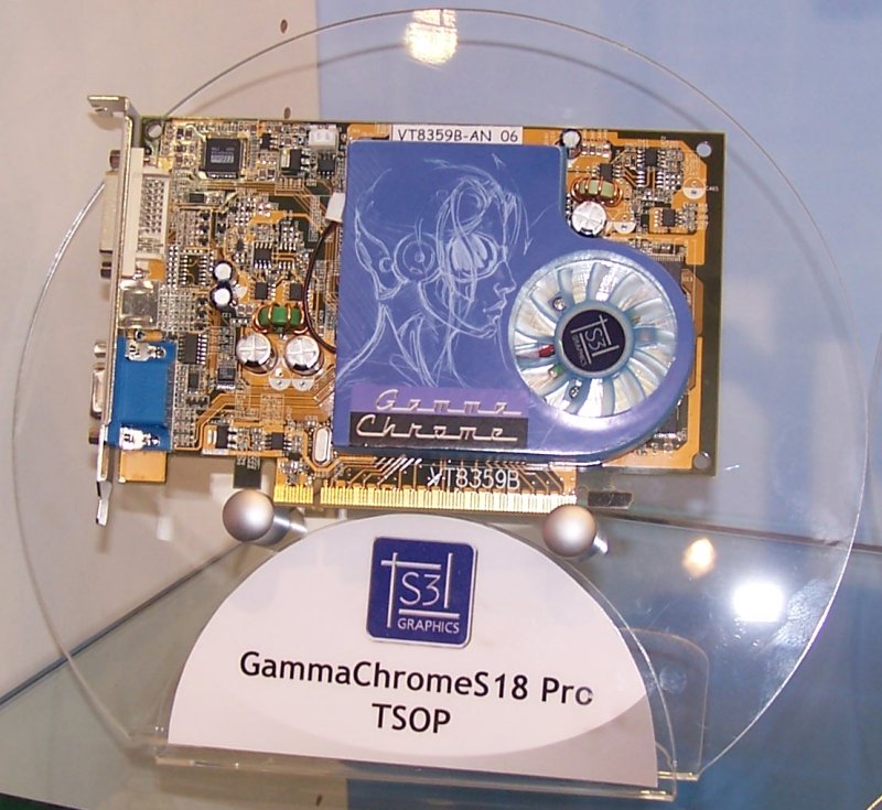
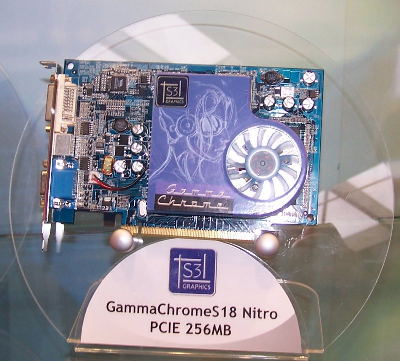
S18 is a 130nm PCI Express chip that features four pixel piplines, each with a single texture sampler and PS2.0 capable maths ALU, and 4 VS2.0 vertex shader units and is aimed towards ATI’s X600 and NVIDIA’s 6200 (standard) solutions. We’ve learnt that unlike the previous chips, S3 have removed any FP16 instructions and now all the native instructions in the Pixel Shader ALU’s are capable of an FP24 precision instruction on a single cycle so that full precision ops on S18 run at the same speed as partial precision ops on their previous DX9 chips. S3 say that they have made other improvements to the S18 chip in relation to the DeltaChrome series, such as improving the early Z reject capabilities.
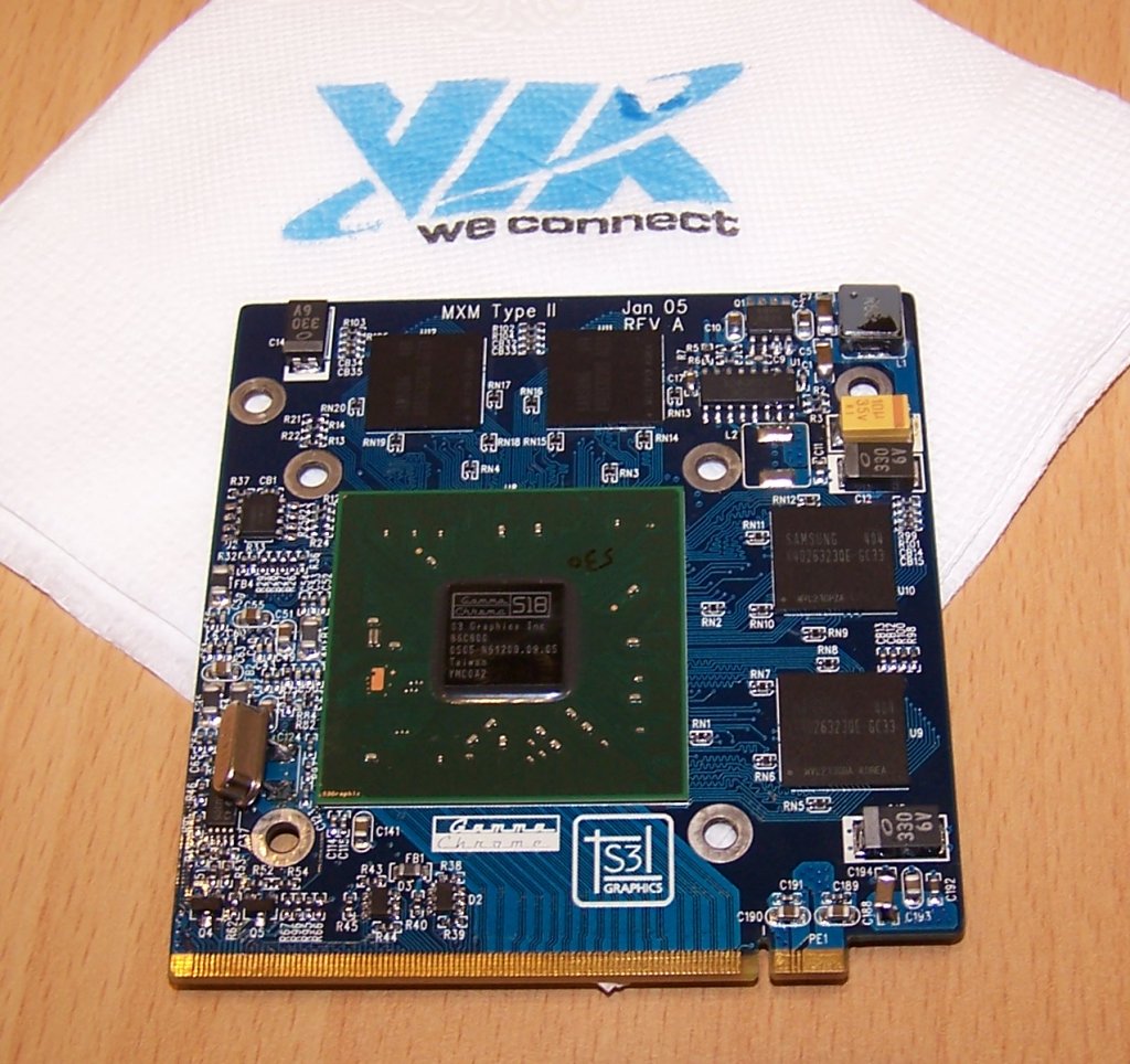
S3/VIA will be aiming the S18 chip at multiple markets and have already designed a notebook variant based on one of NVIDIA’s MXM module designs. They will also specify a "ULP" (Ultra Low Power) version that should at the least be able to run with a passive heatsink, or potentially no heatsink at all.
Later in the year S3 will also be bringing another PCI Express chip, S19, again based on the DirectX9 Shader Model 2.0 standard. Whilst at CeBit VIA had a press conference in which they stated they were due to begin production utilisation on the 90nm node in the second half of the year and given this is when the next generation graphics part is scheduled to hit it would be reasonable to assume that this will be 90nm as well. At present it looks like the chip will have double the pipelines of S18 and be aimed at the higher end of the X700/6600 performance levels.
Beyond S19 S3 have decided to eschew Shader Model 3.0 entirely and instead force ahead with designs for WGF 2.0’s Shader Model 4.0 platform. The name "Destination Films" has been floating around in relation to S3 and this refers the their SM4.0 architecture.