The GeForce 8800 GTX Reference Board
NVIDIA are announcing GeForce 8800 GTX and GeForce 8800 GTS on launch day, and it's the GeForce 8800 GTX we focus on as a means to get you introduced to what the boards are like. GTX is definitely the full-fat version, GTS scaling down not just in G80 configuration but also board form factor.
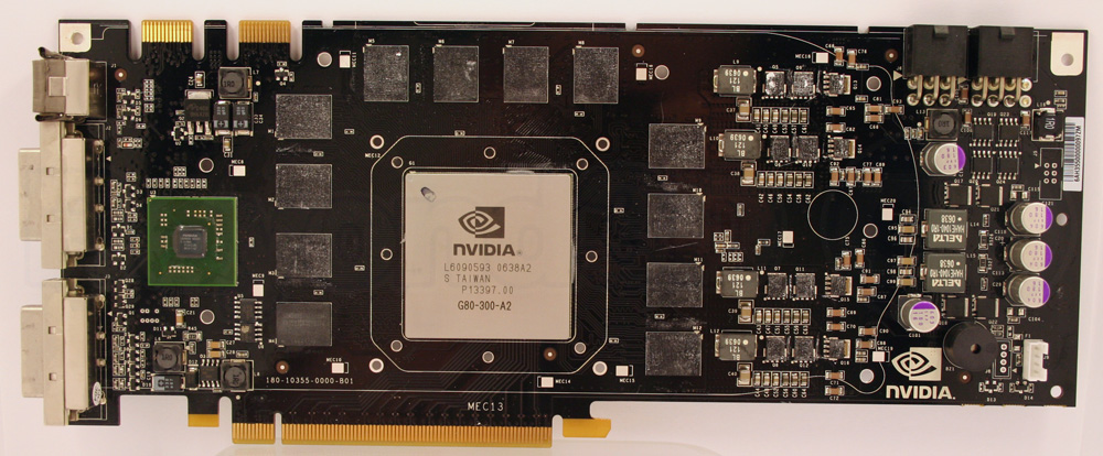
We need a slight reengineering of our 3D tables to completely account for the fact that G80 doesn't run the entire chip at the same clock, NVIDIA clocking the shader core at more than twice the rate of the rest of the chip. Official clock rates for GeForce 8800 GTX are 575MHz base clock (bits of the chip front end and ROPs, mostly), 1350MHz (yes, 1.35GHz) shader clock for the majority of the processing hardware, before the back end of the chip communicates with an external memory pool 768MiB in size via a 384-bit 6-channel memory bus. And we know the texture fillrate number is wrong!
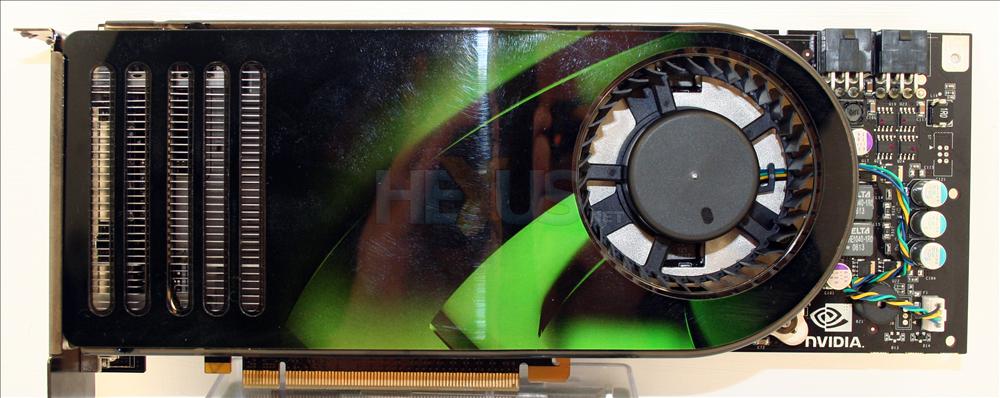
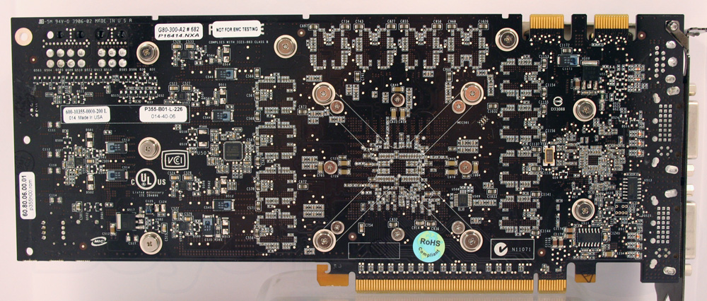
GeForce 8800 GTX products are some 267mm long from backplane to PCB end, carrying dual-slot cooling and dual power inputs (75W each). Weighing 740g, GeForce 8800 GTX is the largest consumer graphics board ever created, the PCB definitely overhanging the edge of any standard 9-hole ATX-spec mainboard by some distance. The side-exit power input connectors are a definite concession to board length, NVIDIA realising that rear-exit would definitely cause GeForce 8800 GTX not to fit in even more cases.
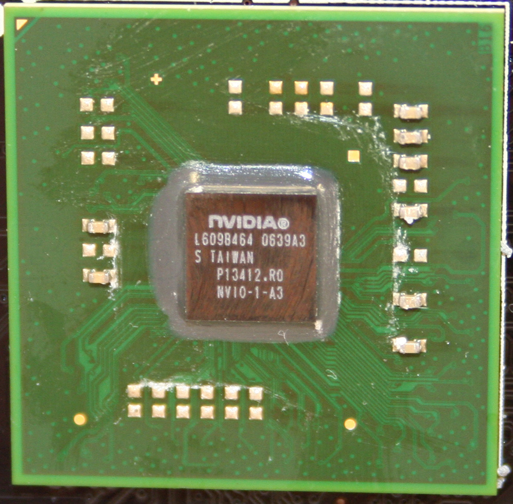
You can also see dual SLI connectors that feed in to NVIO (pictured below), NVIDIA's brand new I/O processor for handling signal input and output to their next generation of GPUs. NVIO marshalls and is responsible for all data that enters the GPU over an interface that isn't PCI Express, and everything that outputs the chip that isn't going back to the host. In short, it's not only responsible for SLI, but the dual-link DVI outputs (HDCP-protected), all analogue output (component HDTV, VGA, etc) and input from external video sources.
Samsung 512Mib DRAMs are used for the memory pool, the DRAM giant's K4J52324QC BJ11 (900MHz) variant chosen for GTX and run at its maximum rated clock. All the DRAM devices are actively cooled by one-piece heatpiped heatsink and fan assembly that also actively cools NVIO, as well as the GPU package and some of the power regulation components at the read end of the board. The cooling assembly is efficient, a large rotary blower-type fan pushing air across the sizable heatsink mass and out of your chassis via the backplane.
Thermally and acoustically the cooler assembly seems to do a sterling job. The heat output from the DRAM pool and the GPU is substantial at times, but the cooler exhausts exchanged heat without any hint of overheating whatsoever, and more impressively at noise levels that are barely higher than the outgoing GeForce 7900 GTX. That product's cooler, one which first made its appearance back on the GeForce 7800 GTX 512, is widely lauded as being the best dual-slot cooler ever used as original equipment. We think that the reference cooler strapped to the GeForce 8800 GTX configuration, which will ship with all initial GeForce 8800 GTX boards from all add-in board partners, deserves similar accolades.
Therefore it's the size of the board and the resulting form factor that will cause most concern. 10.5 inches is a lot of PCB to accomodate in a PC chassis, and some potential customers buying GeForce 8800 GTX as an upgrade or part of a self-build will undoubtedly need a chassis change to get it to fit comfortably as part of the rest of the PC's configuration. While NVIDIA have made very effective use of the available PCB space, such that the PCB is realistically as short as it can be, the requirements for power dictate that board length is an issue. It's the only thing we dislike about the configuration of GeForce 8800 GTX.
Power consumption wise, NVIDIA ask you to connect two 6-pin power connectors simply because the clock rates of the GTX mean that power consumption topping 150W, the maximum possible via one of the standard connectors and the PCI Express slot, can be seen depending on what the board is being asked to do. It's not however a hint that power consumption will get anywhere near 225W. Far from it, infact. Our testing indicates a peak single board consumption of just over 165W, and average power consumption over a range of game tests seems to be no more than any other single board on the market today. The board will shout at you furiously if you don't connect two, however, should you decide you think you can get away with just the one.
Lastly, the G80 on our reference board is A2 silicon, manufactured in week 38 of 2006, inside a chip package a square 42.5mm in size. NVIO is NVIDIA's NVIO-1 revision, A3 silicon and produced in week 39 of 2006. NVIO-1 dice are currently 7x7mm and are produced on TSMC's 110nm value silicon process, packaged as a flipchip with an apparent 553 pins (we haven't counted them, so don't take it as gospel!). Let's document the test setup used for our G80 architecture investigation work, before diving straight into the goodies.