NVIDIA G84 Overview
We ran out a similar diagram for G80, so readers of our initial investigations into that chip should find the following mostly familiar. It omits (crucial) details but should provide a basic overview of the architecture if you're into how a modern GPU works. The diagram assumes that you know that NVIDIA's G8x graphics chips are all heavily threaded, unified and self load balancing.
Sampler threads are scheduled independently of shading threads, the primary ALU structure is fully FP32 and meets international standards for computation and rounding of single precision floats, and the basic architecture is designed around instruction throughput and hiding sampling latency as major design goals. We refer you to the beginnings of our G80 investigation if you want to get the most of the diagram and how we explain how the chip works.
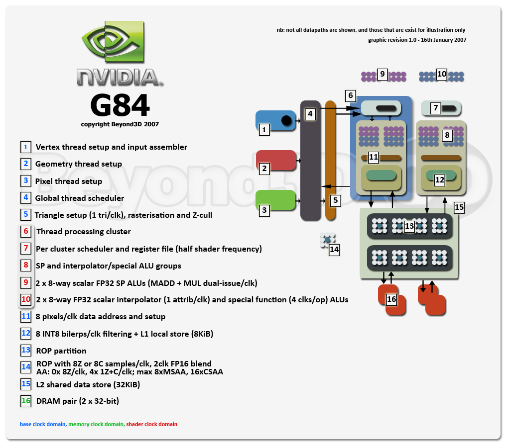
A quick squint at that should give you the basics, so let's take a closer look.