Shader Core
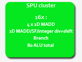
Ah, the processing guts of the beast. With four such clusters, R600 sports a full 320 separate processing ALUs dedicated to shading, with the units arranged as follows. Each cluster contains sixteen shader units, each containing five sub scalar ALUs that perform the actual shading ops. Each ALU can run a separate op per clock, R600 exploiting instruction-level parallelism via VLIW. Having the compiler/assembler do a bunch of the heavy lifting in terms of instruction order and packing, arguably reduces overall efficiency compared to something like G80's scalar architecture that can run full speed with dependent scalar ops. Not all the ALUs are equal, either, with the 5th in the group able to do a bit more than the other four, and independently of those too.
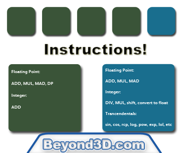
The VLIW design packs a possible 6 instructions per-clock, per-shader unit (5 shading plus 1 branch) into the complete instructions it issues to the shader units, and those possible instruction slots have to match the capabilities of the hardware underneath. Each of the first 4 sub ALUs is able to retire a finished single precision floating point MAD (or ADD or MUL) per clock, dot product (dp, and special cased by combining ALUs), and integer ADD. In terms of float precision, the ALUs are 1 ULP for MAD, and 1/2 ULP for MUL and ADD. The ALUs are split in terms of gates for float and int logic, too. There's no 32-bit mantissa in the ALU to support both, but only one datapath in and out of the sub-ALU, so no parallel processing there. Denorms are clamped to 0 for both D3D9 and D3D10, but the hardware supports inf. and NaN to IEE754 spec.
The fifth fatter unit (let's egotistically call it the RysUnit, since it shares my proportions compared to normal people, and I can be 'special' too) can't do dp ops, but is capable of integer division, multiply and bit shifting, and it also takes care of transcendental 'special' functions (like sin, cos, log, pow, exp, rcp, etc), at a rate of one retired instruction per clock (for most specials at least). It's also responsible for float<->integer conversion. Unlike the other units, this one is actually FP40 internally (32-bit mantissa, 8-bit exponent). This allows for single-cycle MUL/MAD operations on INT32 operands under D3D10, which G80 needs 4 cycles for. It's certainly an advantage of having a VLIW architecture and multiple kinds of units. If you didn't follow that, the following should help.
Each cluster runs thread pairs with the same type in any given cycle, but each of those four clusters can run a different thread type if it needs to. The front-end of the chip handles the thread load balancing across the core as mentioned, and there's nothing stopping all running threads in a given cycle being all pixel, all vertex, or even.....you guessed it: all geometry, although that might not be the case currently. More on that later.
For local memory access, the shader core can load/store from a huge register file that takes up more area on the die than the ALUs for the shader core that uses it. Accesses can happen in 'scalar' fashion, one 32-bit word at a time from the application writer's point of view, which along with the capability of co-issuing 5 completely random instructions (we tested using truly terrifying auto-generated shaders) makes ATI's claims of a superscalar architecture perfectly legit. Shading performance with more registers is also very good, indeed we've been able to measure that explicitly with shaders using variable numbers of registers, where there's no speed penalty for increasing them or using odd numbers. It's arguably one of the highlights of the design so far, and likely a significant contributor to R600's potential GPGPU performance as well.
Access to the register file is also cached, read and write, by an 8KiB multi-port cache. The cache lets the hardware virtualise the register file, effectively presenting any entry in the cache as any entry in the larger register file. It's unclear which miss/evict scheme they use, or if there's prefetching, but they'll want to maximise hits for the running threads of course.
It seems the hardware will also use it for streamout to memory, letting the shader core bypass the colour buffer and ROPs on the way out to board memory, and the chip will also use it for R2VB and overflow storage for GS amplification, making it quite the useful little piece of on-chip memory.
While going 5-way scalar has allowed AMD more flexibility in instruction scheduling compared to their previous hardware, that flexibility arguably makes your compiler harder to write, not easier. So as a driver writer you have more packing opportunities -- and I like to think of it almost like a game of Tetris when it comes to a GPU, but only with the thin blocks and with those being variable lengths, and you can sometimes break them up! -- those opportunities need handling in code and your corner cases get harder to find.
The end result here is a shader core with fairly monstrous peak floating point numbers, by virtue of the unit count in R600, its core clock and the register file of doom, but one where software will have a harder time driving it close to peak. That's not to say it's impossible, and indeed we've managed to write in-house shaders, short and long and with mixtures of channels, register counts and what have you, that run close to max theoretical thoughput. However it's a more difficult proposition for the driver tech team to take care of over the lifetime of the architecture, we argue, than their previous architecture.
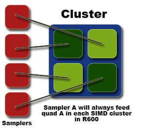
In terms of memory access from the sampler hardware, sampler units aren't tied to certain clusters as such, rather certain positions inside the cluster. If you visualise the 16 shader units in a cluster as being four quads of units, each of the four samplers in R600 is tied to one of those quads, and then across the whole shader core.
And it's the sampler hardware that we talk about next.