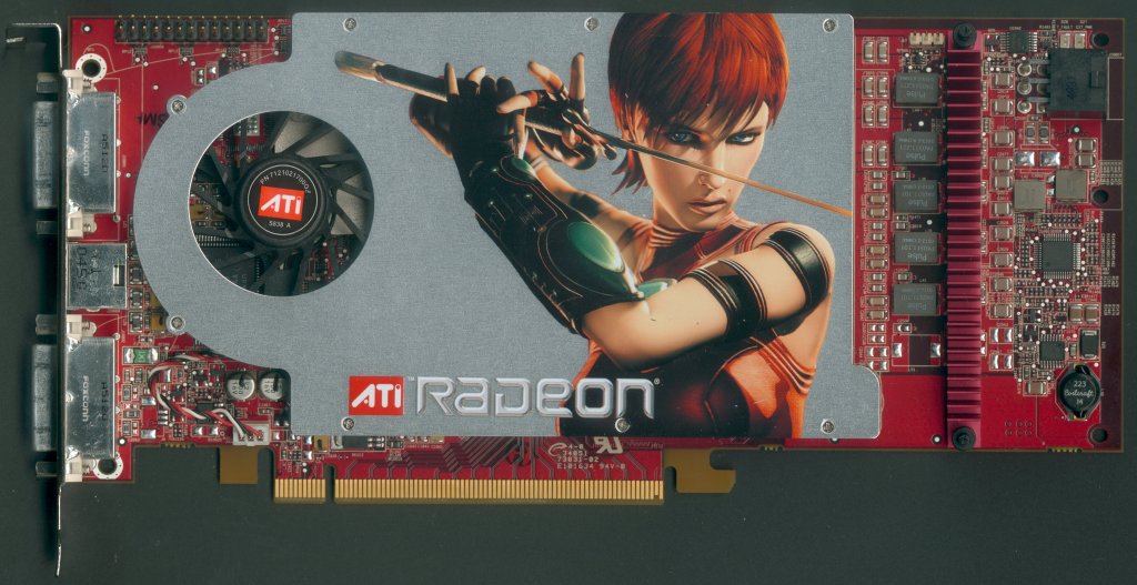
Radeon X1800 XL
The Radeon X1800 XL configuration is the second and, currently, only other configuration the X1800 boards have been announced in, and this represents the entry level to the X1800's.
| Board Details | |
| Board Name | Radeon X1800 XL |
| Core Clock Rate | 500MHz |
| Pixel Pipelines | 16 |
| Pixel Fill-rate | 8000M Pixels/s |
| Texture Fill-rate | 8000M Texels/s |
| Geometry Processor | 8 VS |
| Geometry Rate | 1000M Triangles/s |
| Memory Speed | 500MHz |
| Memory Bandwidth | 32.0GB/s |
| Frame Buffer Size | 256MB |
| Host Interface | PCI Express x16 |
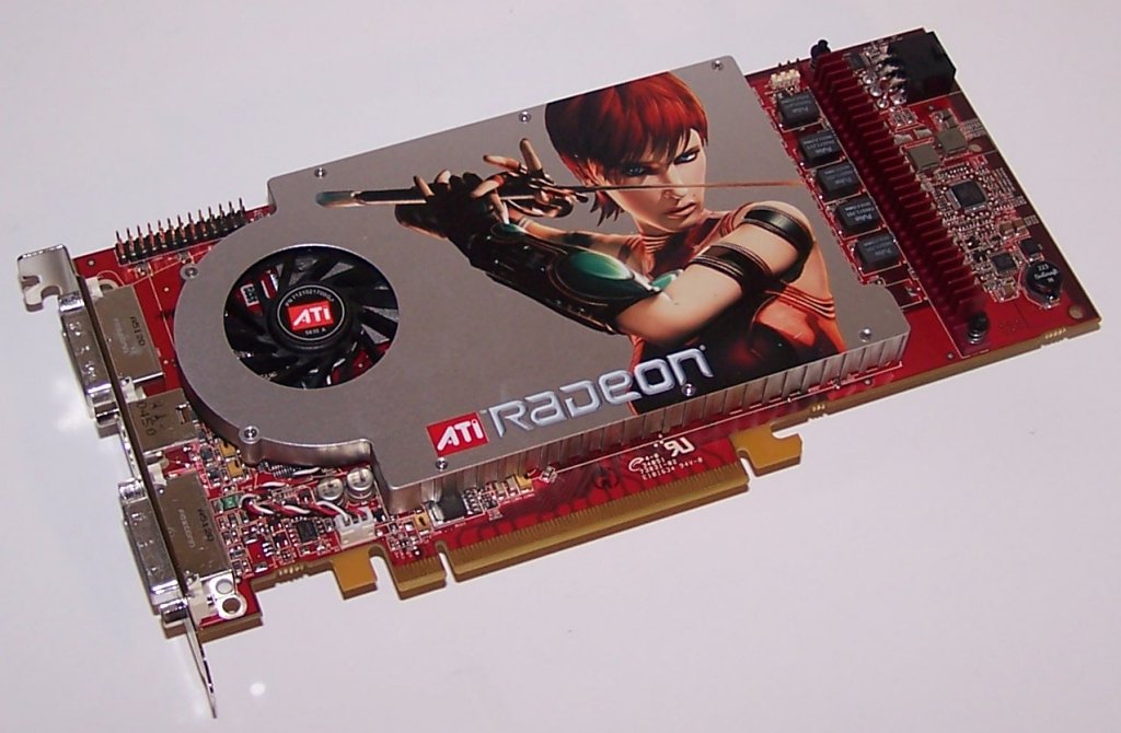
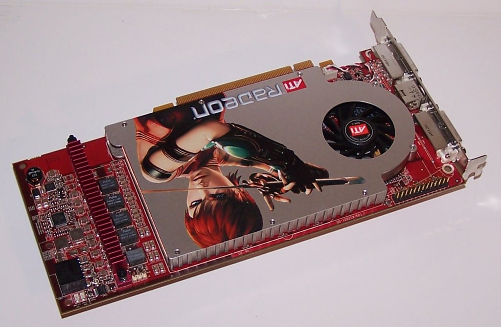
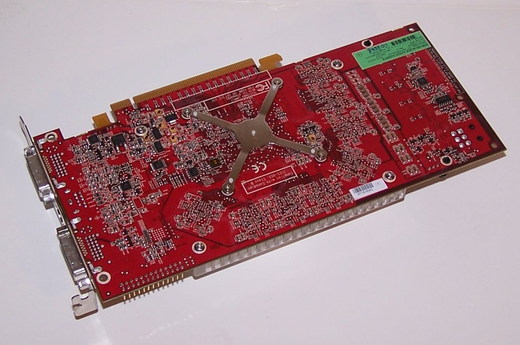
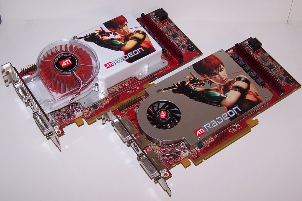
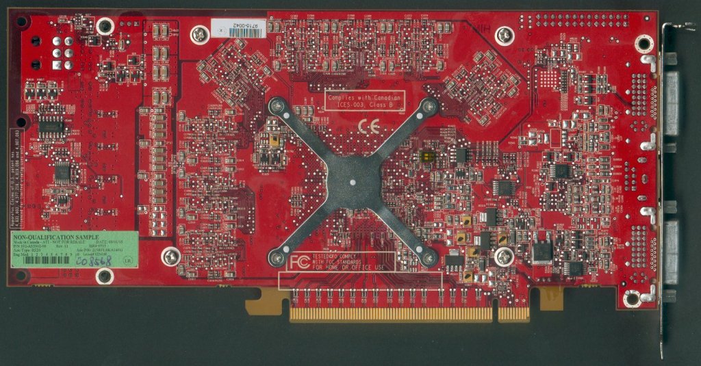
As the specifications show there is a fairly large difference between the X1800 XT and XL boards in terms of clock speeds, with the core dropping 125MHz and the memory 250MHz from the XT to the XL. Because the board isn't running as high clocks this one manages to do with just a single slot cooler and standard fan, although the PCB is still exactly the same. As with the XT, the XL's fan speeds are varied between a number of steps based on the temperature of the core. The XL board has the same level of input/output functionality as the XT, with two Dual-DVI outputs and a video input/output port.
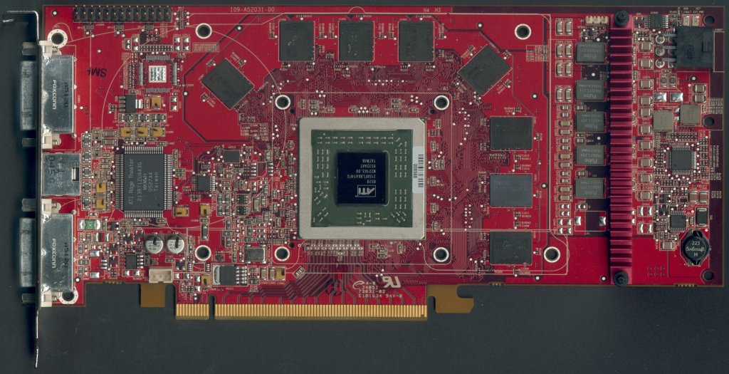
The memory layout of the XL board the same as the XT, and again ATI are using the newer 136 BGA packaged memories, but on this occasion Samsungs K4J55323QG memory is used. The Samsung memory used here are 256Mb, 32-bit chips, so eight modules makes both the 256-bit bus with and the 256MB of local memory. Curiously, the memory on this test sample is rated at 1.4ns, capable of speeds of 700MHz, so ATI are running it considerably under clocked - caution should be advised with expecting this memory on retail products as there are slower memory types that would work and be a closer specification to the XL's speeds.
One thing that can be noticed between the XT and XL boards is that the XL uses an R520 chip revision of A14 and the XT appears to have A15 - the first digit after the "A" represents the silicon revision, while the second signifies the metal layer revision number. Here we can see that the boards are using the same base silicon design, but different metal layers; we are also aware of an A23 revision which indicates that a different silicon revision is also out there. Evidently, when ATI thought they had identified the final issue with the R520 chip they sent three different revisions of, with different changes, to see which cures the problem best - the two chip revisions here represent just two different methods of fixing the issue, but ultimately once they have gone through these wafers just one revision is likely to remain as the production silicon.