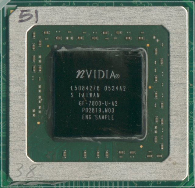
 IntroductionA little less than five months ago NVIDIA launched their latest high end graphics chip, G70. Given the competitive environment at the time, thanks to ATI's R520 misstep, NVIDIA had the luxury of being able to build up stock prior to release and to set, what would now appear to be, reasonably conservative clockspeeds on their flagship GeForce 7800 GTX product, based on the G70 chip. In time for the holiday season, and just as the competitive environment is changing with ATI finally releasing parts of their new X1000 series, NVIDIA is giving their line a little refresh. With the mainstay of their 90nm based line-up yet to come, this pre-Christmas refresh is based on currently available parts moving into new price brackets, but while the lower end gets cheaper the high end gets more expensive - but also gains some fairly significant increases. Here we're taking a look at NVIDIA's new GeForce 7800 GTX 512MB board to see how it has moved on from the previous GTX 256MB configuration. The Graphics ChipThe new GeForce 7800 GTX 512MB board is based on the same G70 chip as the rest of the 7800 series, however NVIDIA are stating that due to some process changes they can now yield the part at higher clockspeeds for this new product. The details of the chip are as follows:
Its interesting to note that the chip is marked as "7800-U-A2" giving an indication to this being a chip speed binned as an "Ultra" part, although NVIDIA ultimately shied away from the name due to the availability stigma attached to it. As the specifications shows, the configuration of this chip is the same as previous parts on the G70 line, and as such the features it enables are the same as well. A quick recap of these capabilities follows:
For a more complete overview of the architecture behind the G70 graphics chip, read our article here. |
|||||||||||||||||||||||||||||||||||
- NVIDIA Fermi GPU and Architecture Analysis
- ATI Cypress Gaming Performance Analysis
- ATI Cypress GPU and Architecture analysis
- ATI RV740 GPU and Architecture Analysis
- NVIDIA GT200 GPU and Architecture Analysis
- Travelling in Style: Beyond3D's C++ AMP contest - WINNER ANNOUNCED
- A speculative look on the Wii U GPU
- Was Harry Potter actually into rendering? Beyond3D's first ever book review
- Andy Keane Interview & Tesla Adoption/Deployment
- Diving into Anti-Aliasing
- Dave Kirk - NVIDIA Tesla Launch
- E3 2011: Behind Closed Doors - Witcher 2 Xbox 360... and a Nurse
- AMD's John Bridgman on Radeon, Linux and Open Source 3D
- Q&A with Visceral's Technical Art Director Doug Brooks on Dead Space 2
- Ian Buck - NVIDIA Tesla Launch
NVIDIA GeForce 7800 GTX 512MB Review - Page 1
Published on 14th Nov 2005, written by Dave Baumann for Consumer Graphics - Last updated: 29th Jul 2007

Page Navigation
Site width adjust
![]()
![]()
Reset width
Privacy Policy