GT200: The Shading Core
GT200 demonstrates subtle yet distinct architectural differences when compared to G80, the chip that pioneered the basic traits of this generation of GPUs from Kirk and Co. As we've alluded to, G80 led a family of chips that have underpinned the company's dominance over AMD in the graphics space since its launch, so it's no surprise to see NVIDIA stick to the same themes of execution, use of on-chip memories, and approach to acceleration of graphics and non-graphics computation.
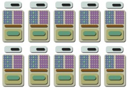
At its core, GT200 is a MIMD array of SIMD processors, partitioned into what we call clusters, with each cluster a 3-way collection of shader processors which we call an SM. Each SM, or streaming multiprocessor, comprises 8 scalar ALUs, with each capable of FP32 and 32-bit integer computation (the only exception being multiplication, which is INT24 and therefore still takes 4 cycles for INT32), a single 64-bit ALU for brand new FP64 support, and a discrete pool of shared memory 16KiB in size.
The FP64 ALU is notable not just in its inclusion, NVIDIA supporting 64-bit computation for the first time in one of its graphics processors, but in its ability. It's capable of a double precision MAD (or MUL or ADD) per clock, supports 32-bit integer computation, and somewhat surprisingly, signalling of a denorm at full speed with no cycle penalty, something you won't see in any other DP processor readily available (such as any x86 or Cell). The ALU uses the MAD to accelerate software support for specials and divides, where possible.
Those
ALUs are paired with another per-SM block of computation units, just
like G80, which provide scalar interpolation of attributes for shading
and a single FP-only MUL ALU. That lets each SM potentially dual-issue
8 MAD+MUL instruction pairs per clock for general shading, with the MUL
also assisting in attribute setup when required. However, as you'll see, that dual-issue performance depends heavily on input operand bandwidth.
Each warp of threads still runs for four clocks per SM, with up to 1024 threads managed per SM by the scheduler (which has knock-on effects for the programmer when thinking about thread blocks per cluster). The hardware still scales back threads in flight if there's register pressure of course, but that's going to happen less now the RF has doubled in size per SM (and it might happen more gracefully now to boot).
So, along with that pool of shared memory is connection to a per-SM register file comprising 16384 32-bit registers, double that available for each SM in G80. Each SP in each SM runs the same instruction per clock as the others, but each SM in a cluster can run its own instruction. Therefore in any given cycle, SMs in a cluster are potentially executing a different instruction in a shader program in SIMD fashion. That goes for the FP64 ALU per SM too, which could execute at the same time as the FP32 units, but it shares datapaths to the RF, shared memory pools, and scheduling hardware with them so the two can't go full-on at the same time (presumably it takes the place of the MUL/SFU, but perhaps it's more flexible than that). Either way, it's not currently exposed outside of CUDA or used to boost FP32 performance.
That covers basic execution across a cluster using its own memory pools. Across the shader core, each SM in each cluster is able to run a different instruction for a shader program, giving each SM its own program counter, scheduling resources, and discrete register file block. A processing thread started on one cluster can never execute on any other, although another thread can take its place every cycle. The SM schedulers implement execution scoreboarding and are fed from the global scheduler and per thread-type setup engines, one for VS, one for GS and one for PS threads.

