Physicals and GeForce GTX 200 Products
Physically
So what about GT200 physically? We need to talk about that before we discuss the products it's going to enable initially, because those physical properties have the most direct effect on board-level metrics like size, power, heat and noise.
NVIDIA won't say exactly how big, but we're pretty confident based on a variety of data that the chip is just about 600mm2 in size, at roughly 24.5mm x 24.5mm. It's built by TSMC on their 65nm major process node, and it's the biggest mass-market chip they've ever produced. It's 1.4 billion transistors heavy, and comes clocked in the same rough ranges that G80 was. We'll note the exact clocks for the two launch SKUs shortly. The wafer shot on page one hints at ~90-95 candidate dice per 300mm start. That's not a lot. We'd call it the Kim Kardashian's ass of the graphics world, but that wouldn't be appropriate for such a sober laugh-free publication as ours.
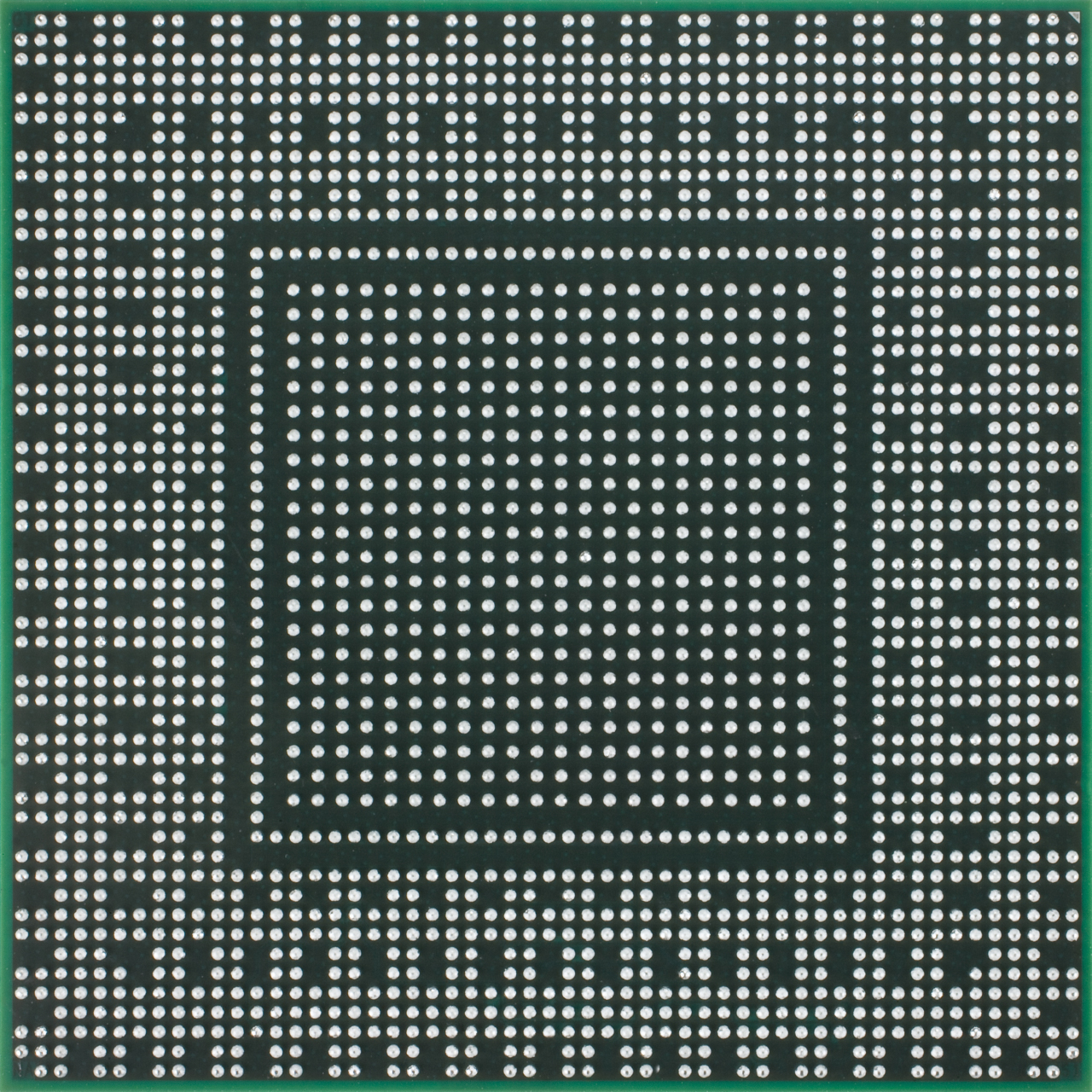
The package for the chip has 2485 pins on the underside as you can see (compared to 2140 on the already massive R600), connecting the processor to the NVIO chip which handles all I/O signalling, power, and the connected DRAMs. A significant portion of the pins are for the power plane, more than the chip needs for I/O and memory connectivity combined.
In terms of clocking, the chip sports more aggressive levels of clock gating, helping GT200 achieve considerably lower idle power draw, at about 25W, than a high-end G92-based product like GeForce 9800 GTX (about 3x higher or so). Interestingly, this clock gating helps keep average power consumption a bit lower than you'd expect given the TDP. The chip also has a dedicated power mode for video playback, turning off a significant percentage of the chip to achieve low power figures when pretty much only the VP2 silicon and NVIO are working.
The chip supports HybridPower, which lets an IGP on the mainboard be responsible for display output when the chip is mostly idle, including when using it to display HD video content via VP2. The potential power consumption savings and noise benefits are quite large, especially in SLI, should your mainboard support a compatible IGP from NVIDIA.
GeForce GTX 200 Series
NVIDIA are redefining the product name and model numbering scheme for GeForce, starting with GT200-based products. The first two SKUs are called GTX 260 and GTX 280, the prefix defining the rough segment of performance and the number the relative positioning in that segment. We wonder if the first digit in the number will denote the D3D class, with 2 correlating to D3D10. GTX 3xx for D3D11 or D3D10.1? We doubt even NVIDIA Marketing knows at this point.
GeForce GTX 280
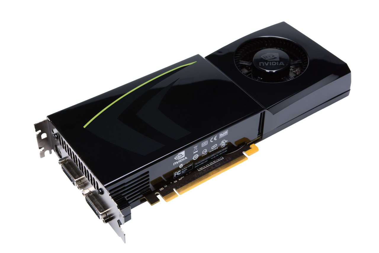
The GTX 280 is the current GT200-based flagship. It uses GT200 with all units enabled, giving it 240 FP32 SPs, 30 FP64 SPs, 512-bit external memory bus and 1024MiB of connected DRAMs. The chip is clocked at 602MHz for the base clock, 1296MHz for the hot clock, and thus 648MHz for the global scheduler. DRAM clock is 1107MHz, or 2214MHz effective.
That gives rise to headline figures of 933Gflops peak FP32 programmable shading rate (1296 x 240 x 3), 77.7Gflops DP (1296 x 30 x 2), 141.7GB/sec of memory bandwidth, 48.16Gsamples/sec bilinear and nearly 20Gpixel/sec colour fill out of the ROPs. The board power at peak is 236W, it requires two power connections, one of them the newer 8-pin standard, with the other the established 6-pin. There's no way to run the board with only 6-pin power, sadly, because of the extra demands on power draw in graphics mode.
The cooler is dual-slot, exhausting air out of the case via the backplane, using a cooler similar to that seen recently with GeForce 9800 GTX, and earlier with GeForce 8800 GTS 512. The backplane sport two dual-link DVI ports, with HDMI possible via active dongle connected to either port. HDTV output via component is supported too, via the smaller 7-pin analogue connector. All GeForce GTX 280s will support HDCP on both outputs, with dual-link encryption.
The board also supports two SLI connectors, for 3-way SLI ability.
GeForce GTX 260
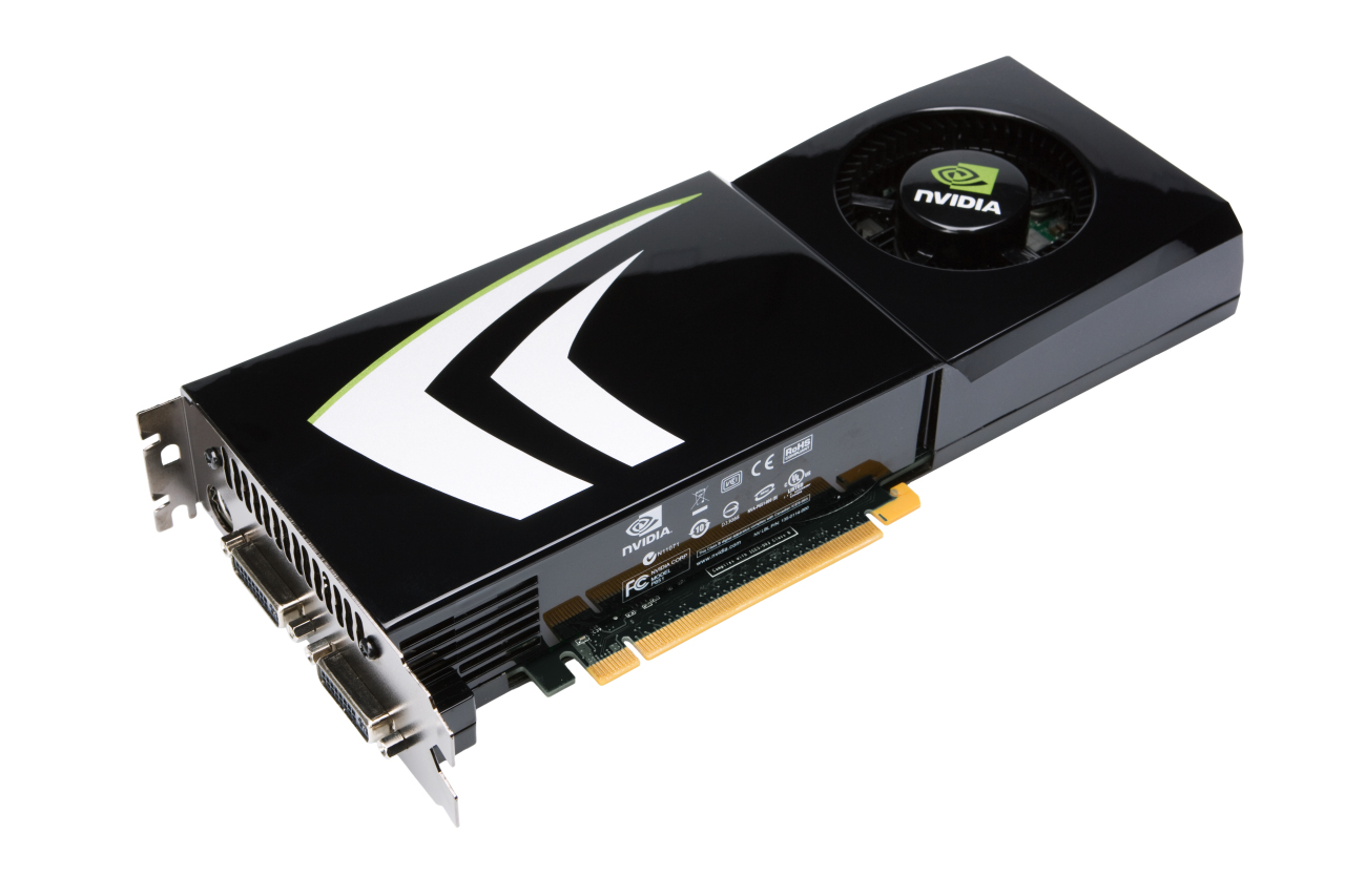
The GTX 260 shares almost identical physical properties, including a very similar PCB and component layout, identical cooler and display output options, and 3-way SLI support. With clocks of 576MHz base, 1242MHz hot, 621MHz global scheduler and 999MHz (1998MHz effective) memory, along with the disabling of two clusters and a ROP channel, the power requirements are lessened. The disabled ROP channel means 896MiB of connected GDDR3.
Peak board power is 182 watts, and power supply is just 2 x 6-pin this time. The clocks give rise to headline numbers of 715Gflops FP32 via 192 SPs, 59.6Gflops DP via 24 FP64 SPs, 111.9GB/sec memory bandwidth via a 448-bit memory interface, 36.9Gsamples/sec bilinear, and 16.1Gpixels/sec colour fillrate out of the ROPs.
Both boards are PCI Express 2.0 native as mentioned, and both sport the VP2 silicon as you know. Our 3D Tables will let you compare to older products to see where things have improved, if you didn't pick it up from the text.