The Reference Board That Ended Up Being Not Quite The Reference
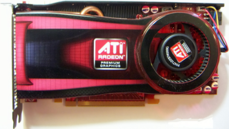
The sample we got from ATI is one of the initial reference design, which means dual-slot cooler and slightly more muscular power delivery circuitry. This hardware revision was intended to be the reference design – we'd be hard pressed to believe otherwise, given how initial briefings were laid out – before the extent of TSMC's 40nm woes was clear. It's our humble opinion that in that particular context, it was no longer economically feasible to sell this card at such a low price-point, since the bad yields increased per-chip costs, and thus a certain amount of cost-cutting had to happen somewhere.
The consequence was that the cards that shipped/are shipping use a slightly simplified layout and have replaced the dual-slot mean-looking cooler with a more tame (and boring, if you ask us) one. However, there are no other functional differences, so the analysis that follows applies to all RV740 based boards. We'll even give you one very good reason for which you shouldn't be too sad over the change.
Before that though, take a look at the nice table below, so that we can discuss it a tad:
Starting near the bottom (don't always do that, unless you're in a rush), you can see that the 128-bit memory interface, when paired with 8 32-bit GDDR5 devices clocked at 800 MHz (3200 MHz effective) satisfy the GPU's needs for acquiring or storing data at a top-rate of 51.2GB/s, which is a bit on the low side when considering the chip's theoretical pixel, zixel and texel generation and processing power. The DRAM comes from the late Qimonda, and is the same flavour that's used on the RV770, rated for a maximum frequency of 1000 MHz (4000 MHz effective). There are about 3 good reasons for which, in spite of using these chips, ATI opted for clocking them conservatively and thus arguably creating something of a bandwidth bottleneck:
- economics – the 4770 SKU is already dangerously close to the 4850, and providing it with more bandwidth might have made it faster, a case in which trouble for the line-up would've ensued, due to the 4850 then becoming a hard sell at its higher price
- thermal and power considerations -- GDDR5 raises some interesting challenges, at least in its current implementation in ATI memory controllers, one being that down-clocking it when idle is not possible in a seamless way (with the exception of the 4870X2, which is a special case by its very nature), so faster DRAM would've meant pushing idle power-consumption and thermal characteristics beyond what the target market considers acceptable
- simplifying PCB design -- this one's rather self explanatory
Speaking of PCBs, and given the fact that these are one of those cases where size actually matters, you should know that for the 4770 boards ATI opted for a 207x98 mm design, which should ensure a simple fit in even the tightest cases. The cooler itself is a mostly aluminium affair, coupled with 2 heatpipes, with air being pushed out by a Delta Electronics BFB1012M blower, for which the spec sheet is available here. Finally, note the 6-pin power connector, added because power consumption under load can reach up to 80W, which overshoots what an accomodating PCI Express slot can provide.
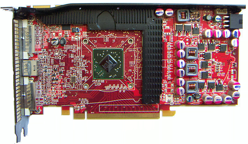
In terms of interacting with the outside world, and propagating its pretty pixels, the card sports two dual-link DVI connectors, each being apt for a sudden transformation into a HDMI output via an included adapter, which quite probably leverages the extra spare pins available on a dual-link DVI connector because the maximum bandwidth required by current HDMI is serviceable using a single DVI link's pins, which is what happens in the scenario we're discussing.