High-level View of RV740
No description of an architecture worth its salt can forego having a general visual representation as its opener. It gets the mental juices flowing and gives much needed basic orientation for the trip that is to come. Given the above, it would've been poor form indeed to avoid drawing this truly artistic depiction below:
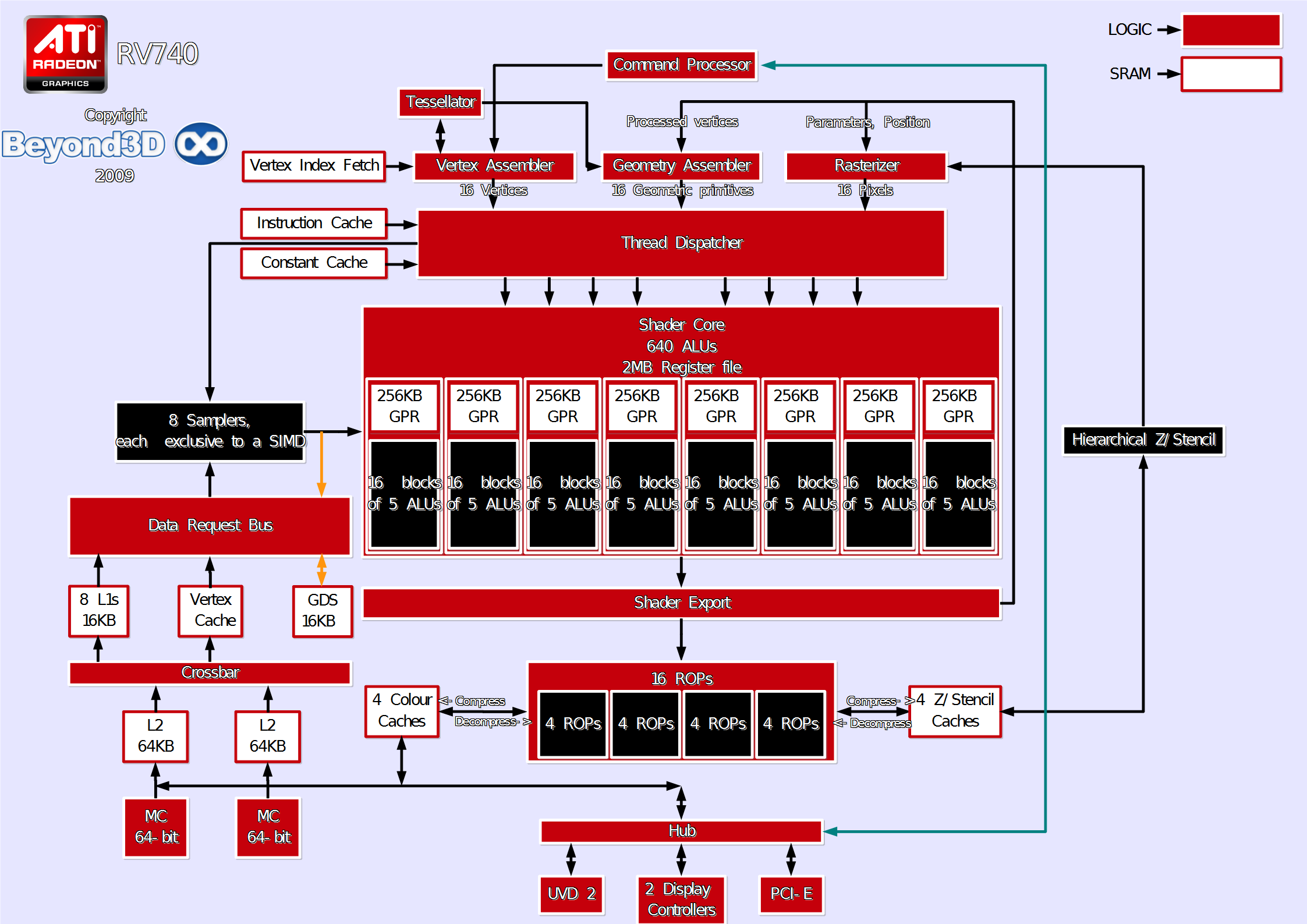
Whilst its artistic merits are easily questionable, its usefulness in telling us what the RV740 is all about is certain: we're dealing with a fully-unified, ALU-dense, fully-threaded auto-balancing architecture. If that sounds somewhat familiar it's because RV740 is an evolution of the base R600 architecture introduced many moons ago, with most of its tenets being respected (albeit not all!).
It's fully DX10.1 compliant, and quite adept at hiding DRAM access latency, as evidenced by the fat register file allowing a very high thread-in-flight count, multi-tiered and spacious cache hierarchy and pretentious dispatch logic -- but more on this later. The only truly sore spot is, as we've already mentioned, the memory interface, which seems quite undersized and inadequate when compared with the rest of the chip.
Discussing the ALUs is a somewhat hairy affair, since they're legion, and not quite equal citizens of the shader-core, with 512 of them being single precision, single cycle MAD capable for floats, and ADD capable for integers (at at basic level). The remaining 128 ALUs (which you'll see called the T-unit here and there) are slightly beefier units adding support for transcendentals, and integer MUL and DIV. Finally, the 512 simpler ALUs can combine in order to perform double precision operations, which results in a 1 MAD per cycle double precision throughput (doubles are represented in a pair of registers and 1 ALU handles the high part, the other the low part). Assuming the colour-scheme used for the diagram hasn't blinded you, hop to the next page.