The Front-end: Command Processor, Setup
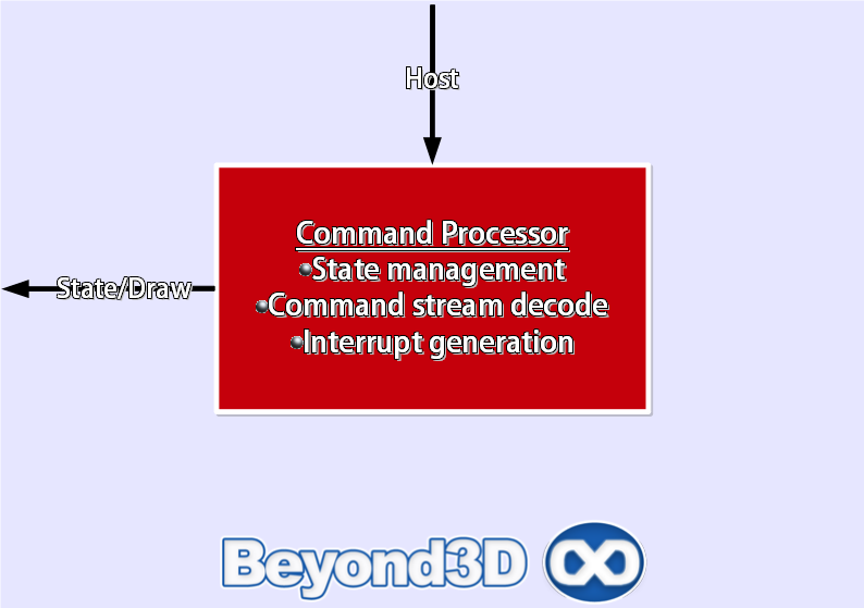
If you were struck by divine inspiration and decided to build your own GPU, the first thing you'd design would be the command processor (CP). This is often neglected when discussing GPUs, with focus falling on ALUs, ROPs, samplers and other more famous blocks -- neglect like that is not necessarily the best approach! The CP is the key to having a good GPU plugged into a waiting PCI Express slot, as opposed to a mere chunk of textolite with some silicon on top. The CP is responsible for fetching and preparing work for the GPU, reporting and scoreboarding of command queue completion, marshalling data, and state management, to name some of its many tasks. Summarising, it's the front-end interface between the GPU and the rest of the system. It's driver-driven, but certainly intelligent in its own right.
For RV740, the CP is a custom RISC based affair, which quite probably is an expansion of the one that was in place for prior R600/RV670 parts, further developed in order to accommodate the increased functional unit count and different sampler blocks. It handles command stream decoding into RV740 specific instructions, possesses full memory read/write privileges and includes multiple command queues, with command streams being fetched via DMA in order to side-step the CPU and decrease latency. Snooping the current state of the GPU's processing units is also possible, in order to avoid needless state switches.
Finally, decoded command streams are passed to logic that handles thread setup, which sets thread type (vertex, geometry, pixel or compute are the possible types) and does data and instruction batching for passing into the setup stage.
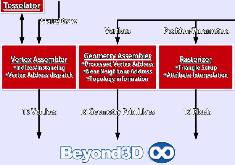
This is another section that hasn't undergone major change from the hardware present in R6 generation chips. The same groups of blocks, matching the corresponding thread type (vertex/geometry/pixel/compute) send 16 objects and related data to the thread dispatcher. There's a slight dichotomy here in that interpolator count has gone up versus the R600/RV670 – but let's not get ahead of ourselves. Typical topology and data flow would imply a progression of the following type, pre-pixel shading: Vertex Assembler->Shader Core->Geometry Assembler->Shader Core->Rasterisation -- for simplicity's sake we're ignoring where data is resident during the process.
As you can see, the tesselator sits on top of the vertex assembler, with which it interacts, receiving the patch to be tessellated, and returning parametric/barycentric domain coordinates for the new tessellated geometry to be passed by the assembler into the shader core. It's there that vertices are evaluated and shaded based on their own data and the initial patch parameters. Both continuous and adaptive tessellation are supported, the level of amplification being controlled per draw call for the former case or through per-edge amplification factors provided in a vertex buffer and fed via R2VB for the latter.
Amplification factors can be either integer or fractional. For R7 generation hardware, and therefore RV740, ATI claims to have tweaked the tessellator by adding interaction with geometry shading. We can only assume, based on how ATI represents the tessellator in its newer presentations, that this means it is now possible to modify the tessellated mesh via a GS program, because verifying it is impossible: at this moment, only the DX9 tessellation libraries and programming examples are available, so the interaction with D3D10+ and OpenGL (and indeed compute, since the tesellator is a legit avenue for compute acceleration) is anyone's guess.
Other than that, and in order to clarify a perhaps foggy topic, the tessellator is not DX11 compliant: it can only amplify up to a factor of 15X – 411 triangles per input triangle – and the hardware needs more to support the new stages in the DX11 geometry pipe, with that stuff only impersonated by multiple, inflexible VS/R2VB passes. For high amplification setup and rasterisation could potentially become a limiting factor.
Picking up where we left off, and skipping over the geometry assembler, let's make the rasteriser the final stop for this page, just like it's the final stop before pixel shading when doing graphics. Triangle setup rate remains unchanged in the RV740 compared to its predecessors, at a steady 1 triangle per cycle, resulting in a grand total of 750Mtris/s at its nominal 750MHz frequency. Vertex attribute fetch rate is also unchanged at a steady count of 16/cycle. Hierarchical Z/stencil and early-Z rejection mechanisms appear to be slightly tweaked, achieving measurably better rejection rates versus the RV670, all else being equal (meaning clocks and bandwidth being aligned).
We'll avoid boring you by detailing for the nth time how hier-Z/S or early-Z rejection work. Attribute interpolation is then performed, with up to 16 pixels/cycle being sent to the thread dispatcher. This time we're going in the same direction since that's the next stop on this trip.