Educated speculations need a modicum of facts
Before starting with the speculation, let’s have a run-down of the facts, just to setup reasonable boundary frames to our wild tech-fuelled imaginations. As soon as Mister Satoru Iwata, President and CEO of Nintendo, took the stage at E3, IBM confirmed, through a press release that Wii U is being built around a custom POWER CPU manufactured on a 45nm process at their East Fishkill facility. Random talks surrounding E3 also brought about some claims, attributed to an IBM spokesperson, that the CPU would carry “a lot” of eDRAM and that its POWER architecture may be related to POWER 7. AMD also confirmed via press release that they were providing a custom GPU for the console. And that’s all we got from Independent Hardware Vendors (IHVs). No mention of clocks, transistor count or any technical details at all. Well, AMD went out of its ways and confirmed that the chip is based on a modern architecture capable of HD graphics. Yeah, thanks for the tip AMD press release! With our starting canvas finally setup, we can start our speculative work.
Wii U: The Facts
| Processor | IBM POWER (Probably POWER 7 based) Multi-Cores 45 nm Process - SOI eDRAM Will be built at IBM East Fishkill (NY, USA) plant |
| Graphics Hardware | AMD custom chip based on a modern and rich core architecture Capable of producing HD graphics |
Wii U: The Unknown (...Reads like a crappy sequel subtitle)
| Processor | Number of cores and hardware threads In Order or OoOE Clock speed Cache setup (L1, L2, L3) |
| Graphics Hardware | Core architecture (RV740, ) Clocks and ALUs setup Number of ROPs eDRAM (yay, nay) Bus(es) width(s) Well, everything really |
| Memory | Amount and clocks Type (DDR3, GDDR3, GDDR5) Bus width (Power is meaningless without cont... bandwidth) Architecture (UMA or NUMA) |
| Misc | South bridge I/O Is Backward Compatibility software only |
The speculation begins... Now!
Since most rumours have it that this GPU, let’s code name it GPU U, derives from RV7x0, we at B3D decided to pick this architecture as our starting point. This would be a reasonably logical evolution, keeping the current component providers and moving up to more recent and higher performing designs. The target for the CPU should be somewhere around or over the X360’s Xenon, which means at least triple core and a comparable clock. The rumour also has it that the mysterious amount of eDRAM available on the CPU wouldn’t only be measured by words like “a lot” but also by number. That number is 16. Being a POWER 7 derivative, the CPU would also be capable of four-way simultaneous multithreading (SMT), whereas the PPC cores of the PlayStation 3 (Cell) and Xbox 360 (Xenon) are only capable of dual-way SMT. If the CPU has indeed 3 cores then, we’d be talking about 12 simultaneous hardware threads, putting an end to Cell’s record of 8 (2 SMT PPC + 6 usable SPUs, one is OS only) in the console space. Although Cell would keep its crown when it comes to concurrent simultaneous hardware threads, with its 7 way heterogeneous SMP setup (1 PPC + 6 SPUs).
Given the nature of this site we’ll spend more time discussing the GPU side of Wii U. We’ll leave the CPU matters, speculative or factual, to our friends at Real World Tech (who also post articles on B3D, but I digress). In any case, focusing on the GPU is good news, because the upgrade is considerably more interesting, since it’s quite literally a quantum leap, from the dark ages of fixed function-ism to the rather posh, DX10.1 levels of programmability. Imagine being frozen back when having hardware T&L was new and fresh and waking up to per-pixel everything, and you have a vague picture of just how big of a jump it’d be. Discerning how that AMD GPU would look is slightly more difficult though, but let’s try it none-the-less.
Before we embark upon the train of speculation, let us walk down the video memory lane and reminisce the RV7xx architecture. AMD, back then ATI, has many a R&D sites where chips are being lovingly etched by master goldsmiths, namely Marlborough, Silicon Valley and Orlando. This latter is where RV7x0 was created by a team led by Scott Hartog. And to continue the name drop streak, Mike Mantor handled the important Shader Core design. Coming a generation after the late to the party and disappointing R6x0, which was beaten to the Unified Shader punch in the PC space by NVIDIA’s G80, RV7x0 had to deliver. And that’s exactly what RV770, the first chip of the series found in the Radeon HD 4870 and 4850 card, did. These great performances coupled to an aggressive pricing kicked start a return to form for the red team -all of that orchestrated under the watchful eye of B3D alumni Dave Baumann acting as the product manager of this series. Many chips and cards followed, making it one of ATI most successful line to date.
Now that we know how RV7x0 came to be and how it fared on the scene and on the market, remains only one important point to cover - the architecture. The point of this article is not to paint every minute details of the architecture, Beyond3D already done exactly that in other articles. Here, we’ll only cover the basics. So, there won’t be talk about crossbar memory bus controller or Super Scalar vector units. We’ll try, at least.
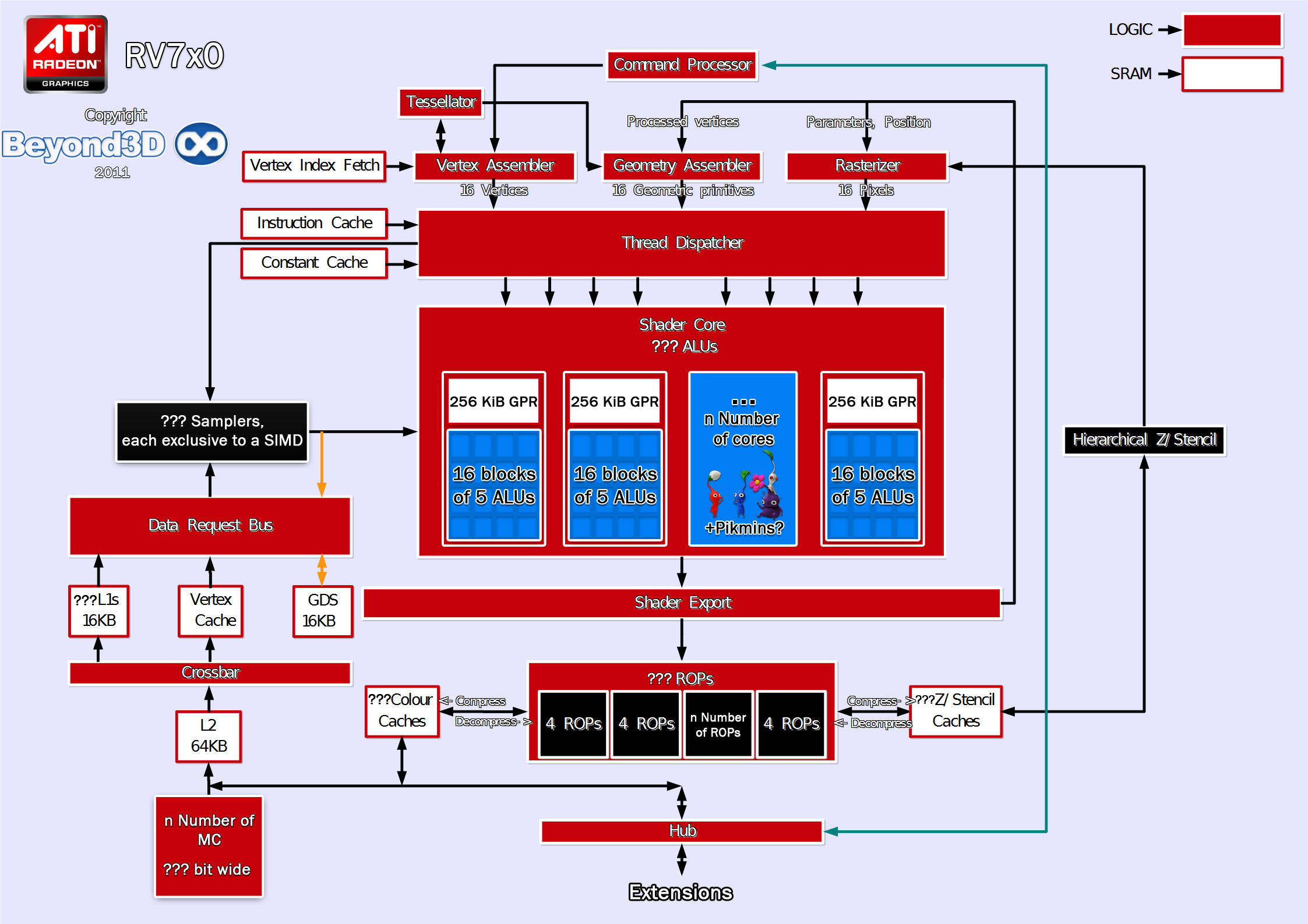
High-level schematic of Wii U GPU architecture
It’s safe to assume that the performance target for the GPU U should be, at least, slightly over Xenos (or C1, Xbox 360 GPU). Casting this into familiar desktop part terms, this means we’re looking for a RV7x0 based configuration that would outperform a 3 SIMD R6xx derivative endowed with wonky ROPs and eDRAM (of course, the differences are more profound, and a straight up 3 SIMD R6x0 part would likely be faster than Xenos in numerous cases). A prime candidate in the RV7x0 family that would fit the bill, in our humble opinion, would be the RV730, probably shrunk to 40nm in order to make it petite enough to be palatable for the target usage case. Such a beast, as is, would have more arithmetic and more texturing capacity than Xenos, with ROP throughput being similar, if we ignore the peculiarities of the eDRAM. Of course, that is what would have been our conservative shot in the dark if the ever churning rumour mill didn’t insist so heavily that the Wii U part will be based on RV740, an architecture we dissected earlier on B3D. However it is worth noting that from a part based on RV740 would be less cost-conscious than RV730 based design, and that is for a number of reasons; chief amongst them being the former’s use of a GDDR5 memory controller (using GDDR3 would be cheaper), its larger size compared to the hypothetical 40nm RV730 and its rather troublesome manufacturing history (TSMC production got better, though). One could argue RV730 should provide Wii U with more graphics throughput than either competing consoles, whilst remaining small and nice. But it goes without saying that a RV740 would be more than welcome to our Beyond3D connoisseur tastes. Note that you should consider the RV730 and RV740 as existing examples, given that the chip that Nintendo will use is a customized derivative, as stated earlier, that is not yet “taped out” (ready for production). In fact, at the present time, from what we heard from sources close to the matter, no close-to-final silicon exists in the wild (development kits) or in the labs yet.