A modular approach to speculative matters
Now that we have settled on that, it would be hard for Nintendo/AMD to produce a chip less capable than Xenos based on the RV7x0 architecture, even if they decide to go for the most humble of the configurations possible; the next step would be to speculate on how much of power that GPU U will be packing? Power in GPU space is a very relative term. Indeed, all ALUs are not equals, all memory buses are not equivalent, not all command processors feed the computing units the same way, not all ROPs process the same amount of pixels, etc. In other words, some parts of a particular chip can be impressive, will other would leave a lot to be desired. So, to prevent any misunderstandings, we’ll target independently a few key sectors of the GPU U, namely the Shader Core, the texture units, the video memory bandwidth and the ROP setup. It’s also noteworthy that each speculated value named reasonable are what we would consider to be the pick of each lists.
To provide some numbers to illustrate our speculation with, we have to set a common variable –namely the GPU clock. We’ll go with 600 MHz for two reasons: first, the golden rule for modern console designs, the thermal design power (TDP) requirements that are intertwined with the form factor of the console. Second, 600 MHz is a good baseline from which a small and efficient console GPU should run at in 2011. To be perfectly thorough, while remaining realistic with our hypothetical scenarios, it could be anything between 600 and 700 MHz.
Other variables such as memory chip frequencies will be follow the same Occam’s razor type of reasonable and/or realistic approach to the speculation.
Shader Core
The Shader Core of a GPU is an architectural concept that didn’t exist in the Wii GPU fixed function era. Back then, the differentiator was the number of “Pipelines,” as generic term used to talk about a vertical slice of the GPU rendering core. In the modern programmable era, where the GPU U sits proudly, the Shader Core of a GPU is the place where the Vertex and Pixel Shader math crushing happens. Simply put, that’s where all the polygons and most of the fancy shaders are produced. In all the various HIV implementations, these cores are always comprised of a string of parallel units known as arithmetic logic units (ALU). These are then grouped in working batches called different names by different companies - nV's shader multiprocessors (whatever nV calls their SIMD arrays), or AMD's SIMDs, etc.)
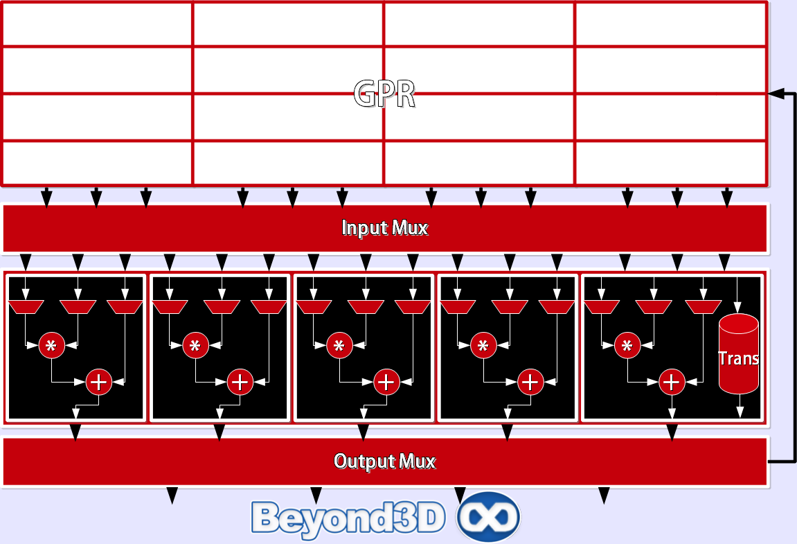
For what it’s worth, RV7x0 Shader Core architecture doesn’t differ from AMD’s more recent architecture like Cypress or Juniper in its setup. They’re all made up of 80 ALUs clusters (16 blocks of 5 ALUs, including one Rys ALU). Cayman, the architecture inside HD69x0 series did bring change to the table, opting for a VLIW4 setup (16 blocks of 4 ALUs). The width and capabilities of these ALUs differ, from a generation to another. Based on that AMD specific granularity of 80 ALUs per cluster, our proposed configurations are the following:
Bare minimum:
240 ALUs – A 3 Clusters setup that would deliver a theoretical (and meaningless, but since we need some scale, that will do) 288 GFLOPS if clocked @600MHz.
In this case, the GPU U wouldn’t have much more processing power than its cousin of the Xbox persuasion, Xenos. In fact, it would have has many ALUs has Xenos. But as we said, not all ALUs are born equals, and the more recent nature of GPU U ones, would give them an edge over Xenos’.
Reasonable entry:
320 ALUs – A 4 Clusters setup that would push 384 GFLOPS @600MHz.
GPU U would mean business. It would easily trump Xenos and RSX (GPU of the PlayStation 3) in any type of calculations whatsoever. Although, it wouldn’t be enough a difference to set the GPU U on a class of its own when compared to the other two. It would beat them, but not outclass them.
High end:
400 ALUs – A 5 Clusters setup rendering 480 GFLOPS @600 MHz
Now you’re playing with power. We’re talking more or less twice the computational power of Xenos and RSX. It would be equivalent to two full PC GPU generation leaps over the current competition.
Top of the line:
800 ALUs – A 10 Clusters – 960 GFLOPS @600 MHz
No graphics programmer in his right mind would qualify GPU U as being “slightly better than Xbox 360.” In fact, that’s the very reason why this scenario can be put to sleep and forgotten.
To give you more food for thoughts and some more perspective, the highest end part AMD built with this type of ALU (VLIW5) had 1600 ALUs and was clocked at 850 MHz. It was the Radeon HD 5870, a hot road that delivered a whooping 2.72 TeraFLOPS. We refer to it as a hot road because it also operated at a TDP, a notion that encompasses power consumption and heat production, that wouldn’t make it a viable choice for Nintendo, or Sony and Microsoft for that matter. But that’s another debate entirely.