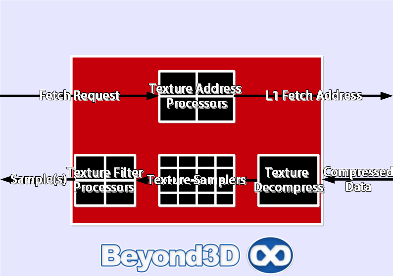
Texture Units – Sampling and filtering
The texture sampling stage, taking place inside the aptly named Texture Units, in a modern rendering pipeline happens at different times. It’s used for texture mapping, of course, but also important for a lot of Shader effects that use texture lookups to a certain end. These texture units perform another important function - filtering. Bilinear, Trilinear, Bicubic, Anisotropic (1x-16x), you name it, are examples of the various hardware accelerated filters available on RV7x0 and up. The speed and number of Texture Units also guarantees that in-surface rendering are benefiting from quality linear filtering. More than that, it also ensures the usability one of the most fundamental tool used in the quest to pristine image quality: anisotropic filtering (AF). A Texture Unit starved design, would be nothing short of a disaster for the image quality and the complexity of some shaders on the GPU U. It is important to keep in mind one of the main differences that the RV7xx series introduced by rapport with its ill fated predecessor: TUs and SIMDs form an unholy union! No longer decoupled, their count scales in tandem, and whilst it would not be impossible for Nintendo to use a custom design that abides by this rule, we're willing to eat a large, tasty, hat, if that happens. Given that context, our prior speculation about the ALU count leads to the following potential TU counts:
Bare minimum:
12 Texture Units – For a texture fillrate of 7200 Mega Texels/Sec @ 600 MHz
Commentary for this part of the GPU U can be summarized by saying that even in the worst case scenario, the TUs will be miles ahead of what’s found in the current consoles.
Reasonable entry:
16 Texture Units – For a texture fillrate of 9600 Mega Texels/Sec @ 600 MHz
High-end:
20 Texture Units – For a texture fillrate of 12000 Mega Texels/Sec @ 600 MHz
Top of the line:
40 Texture Units – For a texture fillrate of 24000 MegaTexels/Sec @ 600 MHz
Going beyond the sterile count, we must also account for the fact that these TUs are architecturally superior to the rather dinky ones found in Xenos, at least in terms of efficiency and cache architecture (we're not even considering RSX here, since that's pretty much a glorified rasterizer / filler of G-Buffers these days).
Render Output Units (AKA ROPs) and Memory interface
The ROPs logic of a GPU is the part that handles the resolve and blending of the pixels into a buffer. The most common type of buffer related to ROPs is the frame buffer, simply put the image that get out of the GPU and displayed onto the screen. You’re currently watching a frame buffer! …Unless of course, you decided to print this article. The ROPs are also the place where one of the most important image-quality related operations takes place: the multi sampling anti-aliasing (MSAA) The number of available ROPs, at a given clock speed, dictates the number of pixel you can output to the screen at any given moment. It dictates how fast you can write those pixels that have been shader coated in the Shader Core to memory - assuming the memory bus and speed are not a bottleneck.
That last assumption brings the other angle to the act of pixel committing pixels to memory: the available memory bandwidth. To get a lot of video memory bandwidth, you are stuck with two options. The first option, what we have on high-end PC part, is to have large bus, and tons of discrete memory chips and thus channels. The obvious downside to this solution is the huge cost associated with having a larger bus, a much more complex PCB layout to accommodate all these memory chips and obviously the chips themselves. The other solution, the one Nintendo used with the GameCube and Wii, is to have the memory used by the ROPs embedded (eDRAM) into the GPU itself (the ROP part at least. Ref. Xenos). No more complex PCB, tons of chips or wide memory bus to deal with. But now, you’re left with two new problems. First, the GPU side silicon cost of this eDRAM, transistors used for eDRAM are transistor that are not used to the computational part of the chip. Second, you now have a very limited amount of ROPs related buffer sizes. The second problem could be taken care of by having recourse to tiling and copying to system memory. That is what happens on Xenos. But as we saw on Xbox 360, tiling doesn’t come free and many developers do not bother with it. Of course, Nintendo could opt to have enough eDRAM to accommodate a 1920x1080 + 4xMSAA buffer, but that would just make problem 1 worse.
We did not consider another way for this memory bandwidth problem. That it could simply be a shortcoming of the architecture. It happened before, for instance, both the original Xbox and PS3 went with an architecture that neither had eDRAM or a lot of RAM chips and a wide video bus. The outcome in both cases was that blending operations, especially Alpha-Blending ones (transparencies), were very costly. Same tune with MSAA.
So here are the proposed scenarios
Bare minimum:
8 ROPs – 128 bit Memory bus – For a theoretical pixel fill rate of 4800 Mega Pixels/Sec @ 600 MHz
If Nintendo goes with the cheaper GDDR3 then: The memory bandwidth will be 28.8 GiB/sec @900 MHz
If Nintendo goes with the newer GGDR5 then: The memory bandwidth will be 57.6 GiB/sec @1800 MHz
With only a meagre 28.8 GiB/sec available, the Wii U will struggle in the same field the Xbox (1) and PS3 struggled before (Alpha Blending, MSAA). These issues would be greatly alleviated in the case of Wii U GPU having a bandwidth of 57.6 GiB/sec when rendering at 720p.
Reasonable entry:
8 ROPs – 16 MB of eDRAM - For a theoretical pixel fill rate of 4800 Mega Pixels/Sec @ 600 MHz
Now, we’re facing a conundrum of sort, in order to calculate the bandwidth of the eDRAM we’d have to know a lot of variables. But principally, we would have to know the actual nature of the interconnection that exists between that eDRAM and the processing part of the GPU U. Of all the probable scenarios, the most common ones would be:
Fully integrated: a scenario à la PS2/PSP/GC/Wii, in which case the total available bandwidth would be anything from incredible to amazing. This in numbers, if we’re to follow C1/Xenos bandwidth calculations, would be something around 310 GiB/sec @600 MHz. And that would be available to all the GPU.
Daughter die dedicated to the GPU: Well, the only example I know of such a design is from ATI and it’s found in Xbox 360’s C1/Xenos GPU. You can take a gander at Dave Baumann’s article on it, to read more on this configuration. In such a case, the bandwidth available to the ROPs is not correlated to the bandwidth available to the other part of the chip. So, you would end up with an high “internal bandwidth” for all the colour/blending/resolve operation and a reasonable “external bandwidth” for the rest of the chip. And even then, it would depend on whether or not the chip could access the eDRAM for operations other than the ROP related ones. But in any cases, given that blending and resolve tasks are those that require the most bandwidth, the GPU will have more than enough bandwidth for all the alpha blending effects the developers would like to use.
High-end:
12 ROPs – 24 MB of eDRAM - For a theoretical pixel fill rate of 7200 Mega Pixels/Sec @ 600 MHz and for the memory bandwidth see above.
For what it’s worth, none of the Wii U tech demos, namely the Japanese Garden and the Zelda demo showed any form of edge Anti Aliasing. Worse, in Ubisoft’s Ghost Recon demo, we noticed slowdowns when a lot of smoke was on screen and micro stutters each time we fired the gun (the “muzzle flash” effect uses alpha blending). On the one hand, combine these anecdotal findings with the rumour that GPU U is derivative of an AMD PC part, which lacks eDRAM, and one could conclude of a lack eDRAM in GPU U and its having limited bandwidth. On the other hand, the Wii U SDK is still in the early stages, the custom hardware is still a prototype and AMD produced eDRAM solutions for console GPUs (GC, Wii, and Xbox 360), so it would not be far-fetched to expect eDRAM in GPU U. A wide memory interface and large quantity of memory chips, for their part, can safely be ruled out for economical reasons.