New Concepts Behind CUDA, Part 1
The parallel data cache (PDC), also known as "shared memory", is one of the key elements of the G80 architecture that allows for more efficient local synchronisation primitives. Based on our information, it likely also is a key element of NVIDIA's architecture for DirectX 10 Geometry Shader acceleration.
Before we go any further, it might be a good idea to introduce you to the architecture proposed by NVIDIA for G8x and CUDA. It is, amusingly enough, extremely similar in principle to one of the diagrams present in at least one of the NVIDIA patents filed back in late 2003. You can't help but respect (or want to horribly maim!) David Kirk for misleading the entire graphics community about NVIDIA's design choices for so many years.
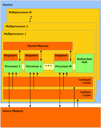
Processors, multiprocessors, and more processors
In G80's implementation of this architecture, there are 8 processors (ALUs) per multiprocessor, and 16 multiprocessors per chip. In our architecture article, we talked in terms of "clusters"; based on this diagram, we can further say that every cluster has 2 multiprocessors in it. Also, as this diagram indicates, it doesn't seem impossible to us that there is at least one register bank per processor.
We would tend to believe that there are 8 independent texture units which work on quads, rather than 16 half-quad units. And considering the multiprocessors are most likely directly linked to texture units, the number of multiprocessors per texture unit has to be an integer. Also remember that those samplers are more capable on the graphics side than they are with CUDA (where you have 64 bilerps/clock of INT8 filtering to burn), since more than bilinear is exposed. More on that later.
Getting back to the diagram, it can be seen that there is one pool of shared memory per multiprocessor. And besides for device memory, there is no way to "communicate" between the different multiprocessors. In fact, no native synchronisation primitives exist to simplify that. This is why we refer to G80's synchronisation functionality as "local" - they do not extend over the entire chip. On the other hand, however, it is incredibly efficient at what it does allow you to do.
So, what exactly is the PDC, anyway? Based on our best understanding of the matter, each block of shared memory represents 16 banks of single-ported SRAM. Each bank has 1KiB of storage and a bandwidth of 32 bits per clock cycle. Furthermore, since there are 16 multiprocessors on a G80, that aggregates to a total storage of 256KiB and bandwidth of more than 675GiB/s. For all intents and purposes, it can be seen as a logical and highly flexible extension of the register file.
In addition to helping for synchronisation, the parallel data cache can always save you bandwidth. The paradigm in this usage scenario is arguably the same as for Cell, where you load data in a SPE's local store manually and then hopefully reuse it several times, minimizing access to DRAM. It is several times smaller, however, but the fundamental idea is the same.
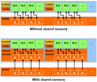
In this completely arbitrary example, only 4 memory reads to DRAM
are required with the parallel
data cache, instead of 6 for previous
GPGPU implementations. This can result in better efficiency
than an
automatic cache, but requires more programmer magic to make it work.
Synchronising execution and data transfers for a larger group of threads isn't exactly 'difficult' either, but it does require explicit synchronisation. So, let's see how that works and what it implies.